Jan 24, 2024
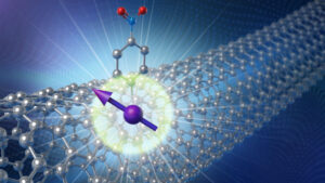
(Tin tức Nanowerk) Researchers with the Department of Energy’s SLAC National Accelerator Laboratory, Stanford University and the DOE’s Lawrence Berkeley National Laboratory (LBNL) grew a twisted multilayer crystal structure for the first time and measured the structure’s key properties. The twisted structure could help researchers develop next-generation materials for solar cells, quantum computers, lasers and other devices.
“This structure is something that we have not seen before – it was a huge surprise to me,” said Yi Cui, a professor at Stanford and SLAC and paper co-author. “A new quantum electronic property could appear within this three-layer twisted structure in future experiments.”
 CAPTION
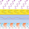
Thêm các lớp, với một sự thay đổi
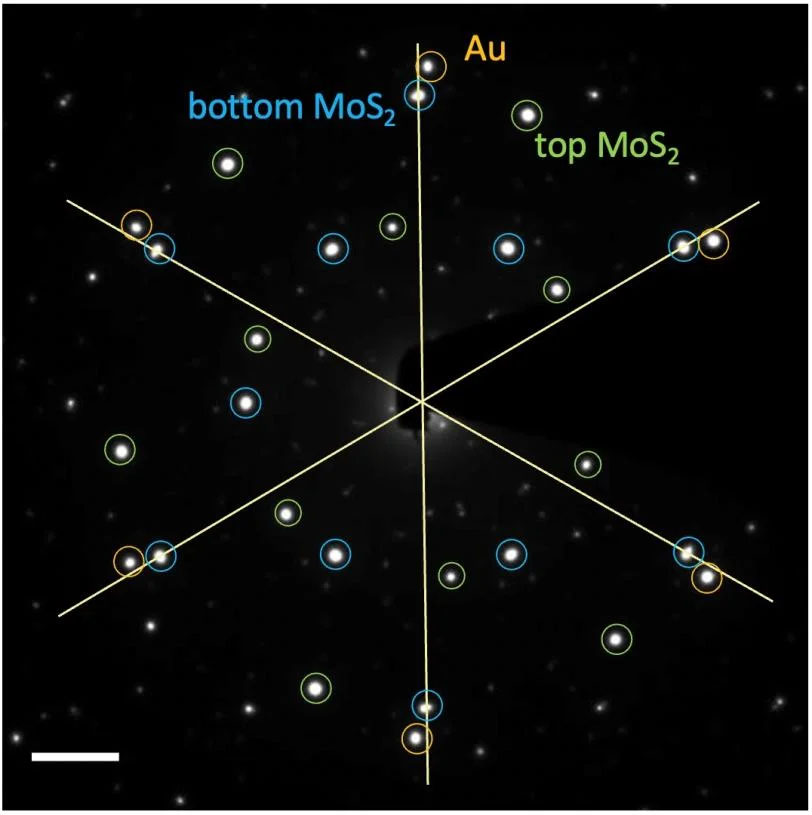
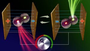
The crystals the team designed extended the concept of epitaxy, a phenomenon that occurs when one type of crystal material grows on top of another material in an ordered way – kind of like growing a neat lawn on top of soil, but at the atomic level. Understanding epitaxial growth has been critical to the development of many industries for more than 50 years, particularly the semiconductor industry. Indeed, epitaxy is part of many of the electronic devices that we use today, from cell phones to computers to solar panels, allowing electricity to flow, and not flow, through them. To date, epitaxy research has focused on growing one layer of material onto another, and the two materials have the same crystal orientation at the interface. This approach has been successful for decades in many applications, such as transistors, light-emitting diodes, lasers and quantum devices. But to find new materials that perform even better for more demanding needs, like quantum computing, researchers are searching for other epitaxial designs – ones that might be more complex, yet better performing, hence the “twisted epitaxy” concept demonstrated in this study. In their experiment, detailed in Khoa học (“Twisted epitaxy of gold nanodisks grown between twisted substrate layers of molybdenum disulfide”), các nhà nghiên cứu đã thêm một lớp vàng vào giữa hai tấm vật liệu bán dẫn truyền thống, molypden disulfide (MoS2). Because the top and bottom sheets were oriented differently, the gold atoms could not align with both simultaneously, which allowed the Au structure to twist, said Yi Cui, Professor Cui’s graduate student in materials science and engineering at Stanford and co-author of the paper. “With only a bottom MoS2 lớp, vàng rất vui khi được căn chỉnh với nó, vì vậy không có hiện tượng xoắn nào xảy ra”, Cui, nghiên cứu sinh cho biết. “Nhưng với hai MoS xoắn2 tấm, vàng không chắc chắn sẽ thẳng hàng với lớp trên cùng hoặc dưới cùng. Chúng tôi đã cố gắng giúp vàng giải quyết sự nhầm lẫn của nó và phát hiện ra mối quan hệ giữa hướng của Au và góc xoắn của MoS hai lớp2".Chuyển đổi đĩa nano vàng
Để nghiên cứu chi tiết lớp vàng, nhóm nghiên cứu từ Viện Khoa học Vật liệu và Năng lượng Stanford (SIMES) và LBNL đã nung nóng toàn bộ mẫu của cấu trúc lên 500 độ C. Sau đó, họ gửi một dòng điện tử qua mẫu bằng kỹ thuật gọi là kính hiển vi điện tử truyền qua (TEM), kỹ thuật này cho thấy hình thái, sự định hướng và biến dạng của đĩa nano vàng sau khi ủ ở các nhiệt độ khác nhau. Việc đo những đặc tính này của đĩa nano vàng là bước cần thiết đầu tiên để hiểu được cấu trúc mới có thể được thiết kế như thế nào cho các ứng dụng trong thế giới thực trong tương lai. Cui, nghiên cứu sinh cho biết: “Nếu không có nghiên cứu này, chúng tôi sẽ không biết liệu có thể xoắn một lớp kim loại epiticular lên trên chất bán dẫn hay không”. “Việc đo cấu trúc ba lớp hoàn chỉnh bằng kính hiển vi điện tử đã xác nhận rằng điều đó không chỉ khả thi mà còn có thể kiểm soát cấu trúc mới theo những cách thú vị.” Tiếp theo, các nhà nghiên cứu muốn nghiên cứu sâu hơn các tính chất quang học của đĩa nano vàng bằng TEM và tìm hiểu xem thiết kế của chúng có làm thay đổi các tính chất vật lý như cấu trúc dải của Au hay không. Họ cũng muốn mở rộng khái niệm này để cố gắng xây dựng các cấu trúc ba lớp bằng các vật liệu bán dẫn và kim loại khác. Bob Sinclair, Giáo sư Charles M. Pigott tại trường Khoa học và Kỹ thuật Vật liệu của Stanford và đồng tác giả bài báo cho biết: “Chúng tôi đang bắt đầu khám phá xem liệu chỉ sự kết hợp vật liệu này mới cho phép điều này xảy ra hay nó xảy ra rộng rãi hơn”. “Khám phá này đang mở ra một loạt thí nghiệm hoàn toàn mới mà chúng ta có thể thử. Chúng tôi có thể đang trên đường tìm kiếm những đặc tính vật chất hoàn toàn mới mà chúng tôi có thể khai thác.”- Phân phối nội dung và PR được hỗ trợ bởi SEO. Được khuếch đại ngay hôm nay.
- PlatoData.Network Vertical Generative Ai. Trao quyền cho chính mình. Truy cập Tại đây.
- PlatoAiStream. Thông minh Web3. Kiến thức khuếch đại. Truy cập Tại đây.
- Trung tâmESG. Than đá, công nghệ sạch, Năng lượng, Môi trường Hệ mặt trời, Quản lý chất thải. Truy cập Tại đây.
- PlatoSức khỏe. Tình báo thử nghiệm lâm sàng và công nghệ sinh học. Truy cập Tại đây.
- nguồn: https://www.nanowerk.com/nanotechnology-news3/newsid=64500.php
- : có
- :là
- :không phải
- 10
- 13
- 14
- 24
- 50
- 50 năm
- 500
- 7
- 8
- 9
- a
- gia tốc
- thêm vào
- thêm
- Sau
- sắp xếp
- cho phép
- Cho phép
- cho phép
- Ngoài ra
- an
- và
- Một
- xuất hiện
- các ứng dụng
- phương pháp tiếp cận
- LÀ
- AS
- At
- nguyên tử
- BAND
- BE
- bởi vì
- được
- trước
- Bắt đầu
- Berkeley
- Hơn
- giữa
- ngũ cốc
- cả hai
- đáy
- thương hiệu
- Brand New
- rộng rãi
- xây dựng
- nhưng
- gọi là
- CAN
- pin
- điện thoại di động
- Tế bào
- C.
- Trung tâm
- Charles
- Đồng tác giả
- kết hợp
- hoàn thành
- phức tạp
- máy tính
- máy tính
- khái niệm
- XÁC NHẬN
- nhầm lẫn
- kiểm soát
- có thể
- quan trọng
- Pha lê
- Ngày
- thập kỷ
- yêu cầu
- chứng minh
- bộ
- Thiết kế
- thiết kế
- thiết kế
- chi tiết
- chi tiết
- phát triển
- Phát triển
- Thiết bị (Devices)
- khác nhau
- khác nhau
- phát hiện
- phát hiện
- DOE
- điện
- điện tử
- điện tử
- năng lượng
- Kỹ Sư
- Ngay cả
- thú vị
- thử nghiệm
- thí nghiệm
- Khai thác
- khám phá
- thêm
- gia tăng
- Tìm kiếm
- tìm kiếm
- Tên
- lần đầu tiên
- dòng chảy
- tập trung
- Trong
- từ
- xa hơn
- tương lai
- Gói Vàng
- tốt nghiệp
- lớn
- Phát triển
- mới lớn
- Phát triển
- Tăng trưởng
- xảy ra
- vui mừng
- Có
- giúp đỡ
- vì thế
- Độ đáng tin của
- HTTPS
- lớn
- if
- hình ảnh
- in
- các ngành công nghiệp
- ngành công nghiệp
- Viện
- Giao thức
- IT
- ITS
- jpg
- Key
- Loại
- Biết
- phòng thí nghiệm
- laser
- lawrence
- lớp
- lớp
- LEARN
- Cấp
- Lượt thích
- quản lý
- nhiều
- vật liệu
- Vật liệu thiết kế
- nguyên vật liệu
- me
- đo
- đo lường
- kim loại
- Kim loại
- Kính hiển vi
- Tên đệm
- Might
- chi tiết
- quốc dân
- Khéo léo
- cần thiết
- nhu cầu
- Mới
- tiếp theo
- thế hệ kế tiếp
- Không
- of
- on
- ONE
- những
- có thể
- mở
- or
- Nền tảng khác
- vfoXNUMXfipXNUMXhfpiXNUMXufhpiXNUMXuf
- tấm
- Giấy
- một phần
- đặc biệt
- thực hiện
- biểu diễn
- hiện tượng
- điện thoại
- vật lý
- plato
- Thông tin dữ liệu Plato
- PlatoDữ liệu
- có thể
- Giáo sư
- tài sản
- tài sản
- Quantum
- máy tính lượng tử
- Tính toán lượng tử
- thực
- thế giới thực
- mối quan hệ
- nghiên cứu
- nhà nghiên cứu
- nhà nghiên cứu
- Tiết lộ
- s
- Nói
- tương tự
- Trường học
- Khoa học
- KHOA HỌC
- tìm kiếm
- đã xem
- bán dẫn
- gởi
- Loạt Sách
- tờ
- đồng thời
- So
- đất
- hệ mặt trời
- Pin mặt trời
- tấm pin mặt trời
- động SOLVE
- một cái gì đó
- stanford
- Đại học Stanford
- Bước
- dòng
- cấu trúc
- cấu trúc
- Sinh viên
- Học tập
- thành công
- như vậy
- chắc chắn
- bất ngờ
- nhóm
- kỹ thuật
- văn bản
- hơn
- việc này
- Sản phẩm
- Tương lai
- cung cấp their dịch
- Them
- sau đó
- Kia là
- họ
- điều này
- Thông qua
- thời gian
- đến
- bây giờ
- hàng đầu
- đối với
- truyền thống
- thử
- xoắn
- hai
- kiểu
- sự hiểu biết
- trường đại học
- sử dụng
- sử dụng
- muốn
- là
- Đường..
- cách
- we
- là
- khi nào
- liệu
- cái nào
- toàn bộ
- với
- ở trong
- thế giới
- sẽ
- năm
- nhưng
- zephyrnet
Thêm từ công trình nano
Các nhà nghiên cứu đã phát triển một phương pháp tự lắp ráp mới để chế tạo các tấm nano 2D nhiều lớp
Nút nguồn: 3088801
Dấu thời gian: Jan 29, 2024
Các khuyết tật spin trong boron nitride hình lục giác được tạo ra bởi quá trình bắn phá ion helium
Nút nguồn: 2782123
Dấu thời gian: Tháng Bảy 24, 2023
Một 'bánh sandwich' cụ thể của graphene và boron nitride có thể dẫn đến vi điện tử thế hệ tiếp theo
Nút nguồn: 2598354
Dấu thời gian: Tháng Tư 20, 2023
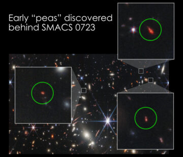
Kính viễn vọng Không gian James Webb tiết lộ liên kết giữa các thiên hà gần và xa
Nút nguồn: 1889333
Dấu thời gian: Jan 9, 2023
Giải phóng một kỷ nguyên mới của các thiết bị nano có thể điều chỉnh màu sắc – nguồn sáng nhỏ nhất từ trước đến nay với các màu có thể chuyển đổi được hình thành
Nút nguồn: 2801585
Dấu thời gian: Tháng Tám 3, 2023
'Làn da' siêu mỏng mới dành cho thiết bị điện tử dẻo hứa hẹn những tiến bộ cho thiết bị y tế và chân tay giả
Nút nguồn: 3075264
Dấu thời gian: Jan 20, 2024
Ống nano carbon là ngôi nhà lý tưởng để quay các bit lượng tử
Nút nguồn: 1995470
Dấu thời gian: Tháng 6, 2023
Dòng điện đi theo một con đường đáng ngạc nhiên trong vật liệu lượng tử
Nút nguồn: 2801583
Dấu thời gian: Tháng Tám 3, 2023
Các oxit phức tạp có thể cung cấp năng lượng cho các máy tính của tương lai
Nút nguồn: 1997462
Dấu thời gian: Tháng 7, 2023
Nguyên tử bất thường giúp tìm kiếm các khối xây dựng của Vũ trụ
Nút nguồn: 1980749
Dấu thời gian: Tháng Hai 24, 2023
Ăng-ten metasurface phổ quát đầu tiên trên thế giới dành cho liên lạc 6G bảo mật cao
Nút nguồn: 3013617
Dấu thời gian: Tháng Mười Hai 14, 2023