Thermal stress is a well-known problem in advanced packaging, along with the challenges of mechanical stress. Both are exacerbated by heterogenous integration, which often requires mingling materials with incompatible coefficients of thermal expansion (CTE).
Effects are already showing up and will likely only get worse as package densities increase beyond 1,000 bumps per chip.
“You combine metals that have a relatively high CTE, then you have polymers that have even bigger CTE stiffness, and then you have dielectrics that have extremely low CTE. Once you put everything together, stress is unavoidable,” said Mario Gonzalez, scientific director and R&D manager for mechanical and thermal modeling and characterization at imec.
Such stress often results in significant warpage or die tilt, which in turn, lead to conditions that diminish reliability. “You’re dealing with different substrate technologies with multiple layer counts,” said Chip Greely, vice president of engineering at Công nghiệp Promex. “Different core thicknesses in substrates, in particular, start to create a lot of classic mechanical problems, including warpage, which has become a pain point for some of the larger players. We’re asking many of our customers who have a system-in-package, heterogeneous integration multi-chip module, to provide the shadow moiré data of their substrates so that we can see the way its warpage changes over reflow temperature and ideally find its reflection point.”
This strain has various negative effects, experienced over many dimensional scales, according to Gilad Barak, vice president of advanced new technologies at Tân tinh. “Often, bending and twisting of features at the nanostructure level results from the built-in stress that has been created, as found in some DRAM and front-end logic nanosheets,” he said. “Another example relates to micron-scale areas where induced strain prevents the fabrication of high-end semiconductor structures, as is typical in ‘keep-out zones’ around through-silicon vias (TSVs). Finally, the large-scale impacts of induced strain can cause wafer bowing, significantly complicating wafer handling and fabrication, which risks fracturing the wafer itself. Wafer bowing is particularly seen during the deposition of thick dielectric layers, as is common during the fabrication of 3D NAND devices.”
The good news is that the industry is very much aware of these and associated problems. The bad news is it’s still short on solutions, although there are many approaches currently being explored.
“There are various methodologies to reduce warpage, but none of them is completely successful, and they always come with tradeoffs,” said Frank Chen, director of applications and product management at Bruker Nano Bề mặt & Đo lường. “The problems are not isolated to a narrow selection of applications. Anytime you attach a die to another substrate, you’re going to have these issues.”
All of this means that inspection and metrology must continue to play critical roles. Other problems, such as hot spots, also can be exacerbated when multiple chips are combined in heterogenous packages.
“During test, various chips will heat up at different times and different temperatures, creating possible hot spots that must be properly cooled, said Andrei Berar, senior director for Test Business Development at amkor. “Besides creating specific thermal active controllers — matching the area of different chips — there are significant efforts to develop adaptive thermal controllers that can ‘anticipate’ the hot spots based on the vectors provided by the test program.”
Such combinations also are leading to increasing use of hybrid metrology – combining different techniques to get to the root of problems most expeditiously.
Design, inspection, test solutions
Indeed, the classic interplay between design, inspection, and thermo-mechanical stress has only gotten more complex with thousands of ever-smaller and more fragile connections.
One result is a renewed emphasis on shifting left, to hopefully “design out” the CTE issues and consequent cascading effects that can lead to overheating and mechanical stress. And to increase the chances of preventing, as well as finding critical defects, simulation and inspection are both needed, according to Andras Vass-Varnai, portfolio development executive with the Electronics and Semiconductor Industry segment of Phần mềm Công nghiệp Kỹ thuật số Siemens.
“Thermal and structural co-simulation using computational flow dynamics (CFD), finite element modeling (FEA), etc., in the early design stage of the package helps both understand the expected performance of the assembly and also allows a good basis for ‘AI driven’ optimization as many of the design choices can be parameterized,” Vass-Varnai explained. “Once the first prototype is built, thermal transient testing can help map the thermal performance of the component. If there is a mismatch between the expected and the real thermal behavior, the test data can be used to ‘calibrate’ the material properties of the package digital twin and update the material libraries for higher initial accuracy of upcoming designs.”
Finding the best way to test bump arrays, and to design for test, is a growing challenge. “What if there’s a signal that goes up and down?” asked Rob Aitken, a Synopsys fellow. “That creates a test problem, because now you’ve got a signal that goes to nowhere and another signal that comes from nowhere, and you have to figure out how you’re going to test those things. Do you probe them? But in that case there’s physical dimensions you have to maintain, and then you run the risk of mechanical damage. Or do you find some kind of JTAG-like structure? But that then reduces the efficiency of these connective points. We’re at the vast experimentation phase where everybody says, ‘Maybe this will work, maybe that will work.’ Right now, I wouldn’t necessarily want to bet on what ‘that’ is.”
There are both indirect and direct test options for defect investigation, according to JCET. For example, CSAM (Computed Scanning Acoustic Tomography) and 3D X-ray are indirect, while mechanical cross-sectional analysis is a tool for direct proof. JCET has advanced thermal characterization equipment to characterize the material/structure issues resulting from mechanical defects, as well.
Optical inspection is, as always, the fastest approach for inline inspection, but best practice is a hybrid approach. “The best method for detecting shorts/opens and marginal defects would be SPI (solder paste inspection) to pre-reflow AOI (automated optical inspection) to post-reflow AOI to inline X-ray,” advised Timothy Skunes, vice president of research and development in Nordson Test & Inspection’s quang học điện tử danh mục đầu tư.
In addition, other modalities may be useful, especially at advanced nodes. For example, a recent approach to characterize strain in semiconductor devices is Raman Spectroscopy (RS). “RS is highly applicable for on-structure measurements, offering rapid measurements on the order of seconds, and small spot sizes of few microns to allow detailed measurements,” said Nova’s Barak. “The difficulty of directly measuring strain on structures prior to the introduction of Raman spectroscopy as in-line metrology tools in the fab led to testing at much later stages in the fabrication process.”
Ultimately, for thorough inspection, there’s no cutting corners. Budget calculations may require comparative metrics, such as the initial cost of a new instrument vs. the ongoing cost of excessive RMAs. And there’s one more thing to consider — how to make sure you can trust your data.
“Are you going to be throwing away what was probably good material to ensure that you don’t have any problem material in what you pass on to the end user? Who’s going to bear the cost of that?” warned Mike McIntyre, director of software product management at Để đổi mới, who recommends a statistical database for accurate comparative assessment when doing automated defect classification.
cong vênh
One of the worst results of stress is warpage. It might be surprising that warpage could be hard to detect, but the effect isn’t always as obvious as it would seem. Warpage causes slight differences in coplanarity between chip and substrate, causing some microbumps to insufficiently connect with pads below, a failure called non-wet.
“Consider an advanced processor that’s 50 to 60mm, as an example,” said Chen. “Because of its large size, it’s challenging to process without any warpage. Nevertheless, if the die-attach tool is tuned the center of its process window, it can pass inspection and be manufactured with high yields. The issue is that the tolerance can be very narrow. As soon as you have a bit of die tilt on on top of the warpage, you have non-wet issues.”
Worse, if this is happening at bump pitches in the 50µm range ( ̴35µm bump size), imagine the issues as bump dimensions shrink further. It’s already a concern for the automotive industry, as it moves toward its next generation in 2023 to 2024. The critical transition will be around the 28nm node, said Chen.
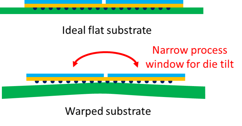
Fig. 1 Die-attach tools have a very narrow process window for die tilt when there is warpage. Source: Bruker
Non-wets
“Non-wets,” is a broad term covering several problems that can occur with solder bumps, most of which are frustratingly subtle. Because solder is often in a liquid state, the process of applying it has been dubbed “wetting.” Tenuous links are called “non-wets,” which are becoming more of a challenge at smaller nodes with thinner connections.
Non-wets often escape typical screening processes, only to show up later as returned chips (RMAs). The root causes can be thermal, mechanical, or a combination, such as thermal cycling in a car that’s also going over rough terrain. The cumulative effect can provide enough thermal-mechanical stress to break the contact.
There are additional nicknames that describe specific types of problems. Instead of the smooth, columnar shape of a good connection, in a “head-in-pillow” defect, one ball seems to sink into the other, like a head on a pillow.
“It’s still making contact so the electrical test can be good, but you can see it’s very fragile,” said Chen, pointing to the X-ray of a head-in-pillow. “As soon as you have some thermal stress or mechanical stress, it might break completely. Even if it is a contact non-wet, the thin connection leads to high-resistance, sub-optimal performance, and likely won’t last long. An open non-wet won’t work at all. In a typical scenario with die tilt, there is a visible transition from well-formed bumps to non-wets.”
The critical issue is latent defects — connections that are functional enough to pass electrical test but fail in the field.
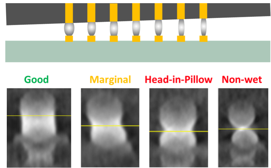

Fig. 2 Gradual transition form good bumps to non-wets in the presence of die tilt. Source: Bruker
“It’s a big issue right now with many types of devices due to the effects of thermal stress,” said Chen. “One customer had product that passed e-test screening and was shipped out. Unfortunately, they had a lot of RMAs due to non-wets failures that developed afterward.”
Some companies are addressing this through painfully tedious manual inspections. Unfortunately, any human examination is subject to operator fatigue, especially when examiners are trying to spot subtle errors during a multi-hour shift.
On the positive side, there are now automated approaches to inspection, such as X-ray tools that can be used inline. “There is a large driver toward high-speed, fully-automated inspection to achieve <100dppb, especially for the automotive industry,” said Chen.
It gets more complicated from there. “Notably, solder, the culprit behind many non-wets, is also subject to electromigration,” said Tom Marinis, a principal member of the Laboratory Technical Staff at Draper. “If the current density in a connection between a chip and substrate is too high for a particular solder over a period of time, because the melting temperature of the solder may be relatively low compared to the operating temperature of the device, you can get migration of the atoms and actually form voids and eventually open up a connection.”
Marinis warned that commercial modeling tools at the device-PCB level aren’t quite mature enough to consistently alert to potential electromigration problems, so it’s important to still perform an accelerated aging test.
Kết luận
Ultimately, detecting reliability issues from latent defects will require higher sampling metrology that is sensitive to die shift, rotation, height, tilt, and other parameters. It also will necessitate more reliance on multi-physics modeling to try to anticipate and resolve potential problems before production. And as the semiconductor and automotive industries continue to intermingle, there’s far more at stake than just RMAs.
“The cost of failure grows exponentially as latent defects pass from devices to modules to cars that could endanger people’s lives,” said Chen. This is why chipmakers are creating holistic solutions that combine design, inspection, and testing to better catch latent faults.
- Phân phối nội dung và PR được hỗ trợ bởi SEO. Được khuếch đại ngay hôm nay.
- Platoblockchain. Web3 Metaverse Intelligence. Khuếch đại kiến thức. Truy cập Tại đây.
- nguồn: https://semiengineering.com/bump-reliability-is-challenged-by-latent-defects/
- 000
- 1
- 2023
- 2024
- 3d
- a
- tăng tốc
- Theo
- chính xác
- chính xác
- Đạt được
- hoạt động
- thực sự
- Ngoài ra
- thêm vào
- giải quyết
- tiên tiến
- Lão hóa
- Cảnh báo
- Tất cả
- cho phép
- Đã
- Mặc dù
- luôn luôn
- phân tích
- và
- Một
- dự đoán
- áp dụng
- các ứng dụng
- Nộp đơn
- phương pháp tiếp cận
- cách tiếp cận
- KHU VỰC
- khu vực
- xung quanh
- hợp ngữ
- thẩm định, lượng định, đánh giá
- liên kết
- đính kèm
- Tự động
- ô tô
- ngành công nghiệp ô tô
- Bad
- banh
- dựa
- cơ sở
- Ghi
- bởi vì
- trở nên
- trở thành
- trước
- sau
- được
- phía dưới
- BEST
- Đặt cược
- Hơn
- giữa
- Ngoài
- lớn
- lớn hơn
- Một chút
- Nghỉ giải lao
- rộng
- ngân sách
- xây dựng
- được xây dựng trong
- kinh doanh
- phát triển kinh doanh
- gọi là
- Có thể có được
- xe hơi
- xe ô tô
- trường hợp
- Catch
- Nguyên nhân
- nguyên nhân
- gây ra
- Trung tâm
- CFD
- thách thức
- thách thức
- thách thức
- thách thức
- tỷ lệ cược
- Những thay đổi
- đặc trưng
- chen
- Chip
- Snacks
- lựa chọn
- cổ điển
- phân loại
- kết hợp
- kết hợp
- kết hợp
- kết hợp
- kết hợp
- Đến
- thương gia
- Chung
- Các công ty
- so
- hoàn toàn
- phức tạp
- phức tạp
- thành phần
- Liên quan
- điều kiện
- Kết nối
- liên quan
- Kết nối
- Hãy xem xét
- liên lạc
- tiếp tục
- Trung tâm
- góc
- Phí Tổn
- có thể
- bao gồm
- tạo
- tạo ra
- tạo ra
- Tạo
- quan trọng
- Current
- Hiện nay
- khách hàng
- khách hàng
- cắt
- dữ liệu
- Cơ sở dữ liệu
- xử lý
- mật độ
- mô tả
- Thiết kế
- thiết kế
- chi tiết
- phát triển
- phát triển
- Phát triển
- thiết bị
- Thiết bị (Devices)
- Die
- sự khác biệt
- khác nhau
- Khó khăn
- kỹ thuật số
- sinh đôi kỹ thuật số
- kích thước
- trực tiếp
- trực tiếp
- Giám đốc
- làm
- dont
- xuống
- vải nỉ
- trình điều khiển
- được mệnh danh là
- suốt trong
- động lực
- Đầu
- hiệu lực
- hiệu ứng
- hiệu quả
- những nỗ lực
- Thiết bị điện tử
- nhấn mạnh
- Kỹ Sư
- đủ
- đảm bảo
- Trang thiết bị
- lỗi
- đặc biệt
- vv
- Ether (ETH)
- Ngay cả
- cuối cùng
- tất cả mọi thứ
- ví dụ
- điều hành
- mở rộng
- dự kiến
- kinh nghiệm
- Giải thích
- Khám phá
- theo hàm mũ
- cực kỳ
- FAIL
- Không
- nhanh nhất
- mệt mỏi
- Tính năng
- đồng bào
- vài
- lĩnh vực
- Sung
- Hình
- Cuối cùng
- Tìm kiếm
- tìm kiếm
- Tên
- dòng chảy
- hình thức
- tìm thấy
- từ
- bực bội
- chức năng
- xa hơn
- thế hệ
- được
- Đi
- đi
- tốt
- dần dần
- Phát triển
- Phát triển
- Xử lý
- Cứng
- cái đầu
- cao
- giúp đỡ
- giúp
- Cao
- cao hơn
- cao
- toàn diện
- Hy vọng
- NÓNG BỨC
- Độ đáng tin của
- Hướng dẫn
- HTTPS
- Nhân loại
- Hỗn hợp
- Tác động
- quan trọng
- in
- Bao gồm
- Tăng lên
- tăng
- các ngành công nghiệp
- ngành công nghiệp
- ban đầu
- thay vì
- cụ
- hội nhập
- Giới thiệu
- điều tra
- bị cô lập
- vấn đề
- các vấn đề
- IT
- chính nó
- Loại
- phòng thí nghiệm
- lớn
- quy mô lớn
- lớn hơn
- Họ
- lớp
- lớp
- dẫn
- hàng đầu
- Dẫn
- Led
- Cấp
- thư viện
- Có khả năng
- liên kết
- Chất lỏng
- cuộc sống
- dài
- Rất nhiều
- Thấp
- duy trì
- làm cho
- Làm
- quản lý
- giám đốc
- nhãn hiệu
- sản xuất
- nhiều
- bản đồ
- Mario
- phù hợp
- vật liệu
- nguyên vật liệu
- trưởng thành
- max-width
- có nghĩa
- đo
- đo lường
- cơ khí
- hội viên
- Kim loại
- phương pháp
- phương pháp
- Metrics
- Đo lường
- Might
- di cư
- hòa lẫn
- người mẫu
- mô-đun
- Modules
- chi tiết
- hầu hết
- di chuyển
- nhiều
- nano
- nhất thiết
- cần thiết
- tiêu cực
- Tuy nhiên
- Mới
- Công nghệ mới
- tin tức
- tiếp theo
- nút
- các nút
- Rõ ràng
- cung cấp
- ONE
- đang diễn ra
- mở
- hoạt động
- nhà điều hành
- tối ưu hóa
- Các lựa chọn
- gọi món
- Nền tảng khác
- gói
- gói
- bao bì
- Đau
- thông số
- riêng
- đặc biệt
- thông qua
- của người dân
- thực hiện
- hiệu suất
- thời gian
- giai đoạn
- vật lý
- nốt
- plato
- Thông tin dữ liệu Plato
- PlatoDữ liệu
- Play
- người chơi
- Điểm
- điểm
- polyme
- danh mục đầu tư
- tích cực
- có thể
- tiềm năng
- thực hành
- sự hiện diện
- Chủ tịch
- ngăn chặn
- Hiệu trưởng
- Trước khi
- có lẽ
- thăm dò
- Vấn đề
- vấn đề
- quá trình
- Quy trình
- Bộ xử lý
- Sản phẩm
- quản lý sản phẩm
- Sản lượng
- chương trình
- bằng chứng
- đúng
- tài sản
- nguyên mẫu
- cho
- cung cấp
- đặt
- R & D
- phạm vi
- nhanh
- thực
- gần đây
- đề nghị
- giảm
- làm giảm
- phản ánh
- tương đối
- độ tin cậy
- sự phụ thuộc
- gia hạn
- yêu cầu
- đòi hỏi
- nghiên cứu
- nghiên cứu và phát triển
- kết quả
- kết quả
- Kết quả
- Nguy cơ
- rủi ro
- vai trò
- nguồn gốc
- chạy
- Nói
- nói
- quy mô
- quét
- kịch bản
- sàng lọc
- giây
- dường như
- phân khúc
- lựa chọn
- bán dẫn
- cao cấp
- nhạy cảm
- một số
- Bóng tối
- Hình dạng
- thay đổi
- VẬN CHUYỂN
- vận chuyển
- ngắn
- hiển thị
- Tín hiệu
- có ý nghĩa
- đáng kể
- mô phỏng
- Kích thước máy
- kích thước
- nhỏ
- nhỏ hơn
- So
- Phần mềm
- Giải pháp
- một số
- Chẳng bao lâu
- nguồn
- riêng
- Quang phổ
- Spot
- Nhân sự
- Traineeship
- giai đoạn
- cổ phần
- Bắt đầu
- Tiểu bang
- thống kê
- Vẫn còn
- căng thẳng
- cấu trúc
- cấu trúc
- Tiêu đề
- thành công
- như vậy
- thật ngạc nhiên
- Kỹ thuật
- kỹ thuật
- Công nghệ
- thử nghiệm
- Kiểm tra
- Sản phẩm
- Khu vực
- cung cấp their dịch
- Đó
- nhiệt
- điều
- điều
- hàng ngàn
- Thông qua
- Ném
- thời gian
- thời gian
- đến
- bên nhau
- khoan dung
- quá
- công cụ
- công cụ
- hàng đầu
- đối với
- quá trình chuyển đổi
- NIỀM TIN
- XOAY
- loại
- điển hình
- hiểu
- sắp tới
- Cập nhật
- sử dụng
- người sử dang
- khác nhau
- Lớn
- Phó Chủ Tịch
- có thể nhìn thấy
- nổi tiếng
- Điều gì
- cái nào
- trong khi
- CHÚNG TÔI LÀ
- sẽ
- không có
- Công việc
- tệ nhất
- sẽ
- X-quang
- sản lượng
- trên màn hình
- zephyrnet