Fabrication
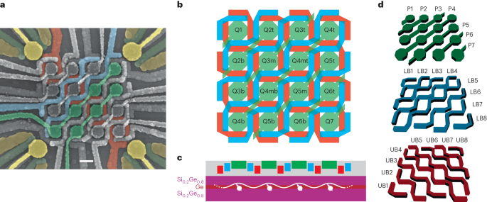
The device is fabricated on a Ge/SiGe heterostructure where a 16-nm-thick germanium quantum well with a maximum hole mobility of 2.5 × 105 cm2 V−1 s−1 is buried 55 nm below the semiconductor/oxide interface25,40. We design the quantum dot plunger gates with a diameter of 100 nm, and the barrier gates separating the quantum dots with a width of 30 nm. The fabrication of the device follows these main steps. First, 30-nm-thick Pt ohmic contacts are patterned via electron-beam lithography, evaporated and diffused in the heterostructure following an etching step to remove the oxidized Si cap layer41,42. A three-layer gate stack is then fabricated by alternating the atomic layer deposition of an Al2O3 dielectric film (with thicknesses of 7, 5 and 5 nm) and the evaporation of Ti/Pd metallic gates (with thicknesses of 3/17, 3/27 and 3/27 for each deposition, respectively). After dicing, a chip hosting a single crossbar array is then mounted and wire bonded on a printed circuit board. Before cool down in a dilution refrigerator, we tested two nominally identical crossbar devices in a 4 K helium bath as per the screening procedure38. Both devices exhibited the functionality of full gates and ohmic contacts, and one of them was mounted in a dilution refrigerator.
Experimental setup
The experiment is performed in a Bluefors dilution refrigerator with a base temperature of 10 mK. From a Coulomb peak analysis, we extract an electron temperature of 138 ± 9 mK, which we use to estimate the detuning lever arm (Supplementary Figs. 12 and 13). We utilize an in-house built battery-powered SPI rack (https://qtwork.tudelft.nl/~mtiggelman/spi-rack/chassis.html) to set the d.c. voltages, whereas we use a Keysight M3202A arbitrary waveform generator (AWG) to apply alternating-current rastering pulses via coaxial lines. The d.c. and alternating-current voltage signals are combined on the printed circuit board with bias-tees and applied to the gates. Each charge sensor is galvanically connected to a NbTiN inductor with an inductance of a few microhenries, forming a resonant tank circuit with resonance frequencies of ~100 MHz. In our experiment, we have observed only three out of four resonances, probably due to a defective inductor. Moreover, because the two resonances overlap substantially, we mostly avoid using reflectometry (unless explicitly stated in the text) and use fast d.c. measurements with a bandwidth of up to 50 kHz. The four d.c. sensor currents are converted into voltages, amplified and simultaneously read by a four-channel Keysight M3102A digitizer module with 500 megasamples s–1. The digitizer module and several AWG modules are integrated into a Keysight M9019A peripheral component interconnect express extensions for the instrumentation chassis. Charge stability diagrams here typically consist of a 150 × 150 pixel scan with a measurement time per pixel of 50 μs. Throughout this Article, we refer to Δgi to identify a ramp supplied by an AWG to the gate gi with respect to a fixed d.c. reference voltage. To enhance the signal-to-noise ratio, we average the same map 5–50 times, obtaining a high-quality map within a minute.
Tune-up details
Throughout the experiment, we have tuned all the 16 quantum dots of the device two times. In the first run, the gate voltages were optimized to minimize the number of unintentional quantum dots to better visualize and characterize the crossbar quantum dots (Fig. 2 and Supplementary Fig. 14). In the second run, the stray dots were neglected to tune the quantum dot array into a global odd-occupation regime (Fig. 3). Between the two tune-up cycles, the gate voltages were reset to zero without thermally cycling the device. The protocol followed in the two tuning procedures was the same, but the need for emptying accidental quantum dots in the first session led to some restrictions in the voltage window of certain gates. The starting gate-voltage values for the tune up are –300 mV for barriers and –600 mV for plungers. In Supplementary Fig. 15, we display the d.c. gate voltages relative to the measurements displayed in Fig. 3, with the crossbar array tuned in the odd-charge occupation. In this regime, we also study the variability in the first hole voltage onset in each dot, obtaining −1,660 ± 290 mV (Supplementary Fig. 16). Furthermore, we characterize the variability in the transition-line spacing to be ~10–20% as a metric for the level of homogeneity of the array (Supplementary Fig. 17)43. Supplementary Note 4 discusses strategies to further reduce these variations.
The odd-charge occupancy is demonstrated by emptying each quantum dot (Supplementary Videos 1–12). All the datasets underlying Fig. 3 and Supplementary Videos 1–12 are taken at the same gate-voltage configuration on the same day. Still, across all the maps, there are minimal voltage differences, the largest being a variation of 6 mV in vP1 that, however, does not affect the Q1, Q2b and Q2t occupancies (Supplementary Table 1). During the experiment, gate UB8 did not function properly, possibly due to a broken lead. To compensate for this effect and to enable charge loading in P3t and P5t dots, we set UB7 at a lower voltage compared with the other UB gates. Additionally, LB1 is set at a comparatively higher voltage to mitigate the formation of accidental quantum dots under the fanout of LB1 and P1 at lower voltages. The first addition line of such an accidental quantum dot is visible as a weakly interacting horizontal line (Fig. 3a).
Virtual matrix
The matrix M defined by (bf{overrightarrow{G}}=M times bf{overrightarrow{{{{rm{v}}}}G}}), with virtual gates (overrightarrow{{rm{v}}bf{G}}) and actual gates (overrightarrow{bf{G}}) is shown as a colour map in Supplementary Fig. 3. For the tunnel coupling experiments presented in Fig. 4, we employ additional virtual-gate systems for achieving independent control of detuning voltages e67 and U67, as well as the interdot interactions via virtual barriers t6b7, j6b7, t6t7 and j6t7. With SE_P defined as the SE plunger gate, we write
$$begin{array}{rcl}left(begin{array}{c},{{mbox{P5}}}, ,{{mbox{P6}}}, ,{{mbox{P7}}}, ,{{mbox{SE_P}}},end{array}right)&=&left(begin{array}{cc}0.04&-1.2 -0.5&0.9 0.492&0.9 -0.08&-0.26end{array}right)left(begin{array}{c},{{mbox{e67}}}, ,{{mbox{U67}}},end{array}right) left(begin{array}{c},{{mbox{P6}}}, ,{{mbox{P7}}}, ,{{mbox{UB5}}}, ,{{mbox{LB7}}}, ,{{mbox{SE_P}}},end{array}right)&=&left(begin{array}{cc}-1.28&-0.33 -1.18&-0.72 1&0 0&1 0.15&-0.01end{array}right)left(begin{array}{c}{{{{rm{t}}}}}_{6{{{rm{t}}}}7} {{{{rm{j}}}}}_{6{{{rm{t}}}}7}end{array}right) left(begin{array}{c},{{mbox{P6}}}, ,{{mbox{P7}}}, ,{{mbox{UB4}}}, ,{{mbox{LB7}}}, ,{{mbox{SE_P}}},end{array}right)&=&left(begin{array}{cc}-2.05&-0.97 -1.18&-0.41 1&0 0&1 -0.19&-0.01end{array}right)left(begin{array}{c}{{{{rm{t}}}}}_{6{{{rm{b}}}}7} {{{{rm{j}}}}}_{6{{{rm{b}}}}7}end{array}right)end{array}.$$
Quantum dot identification
To obtain the capacitive coupling of all the barrier gates to a set of transition lines (Fig. 2b), we acquire and analyse sets of 112 charge stability diagrams. The same charge stability diagram is taken after stepping each barrier gate around its current voltage in steps of 1 mV in the range of –3 to 3 mV (that is, 7 scans × 16 barriers). The number of charge stability diagrams required to identify all the quantum dots scales linearly with their total number. The number of maps results from the product of the number of plungers and barrier gates, both of which scale as its square root. We emphasize that an array with individual control would also require a linear number of charge stability diagrams to infer each dot. In the analysis, we first subtract a slowly varying background to the data (with the ndimage.gaussian.filter function of the open-source SciPy package version 1.7.1) and then calculate the gradient of the map (with the ndimage.gaussian_gradient_magnitude function). For a given linecut of such two-dimensional maps, we extract the peak position using a Gaussian fit function. Due to cross-capacitance, the transition-line positions manifest a linear dependence on each of the 16 barriers, which we quantify by extracting the linear slope (Supplementary Fig. 4). After normalization to the maximum value, these parameters are named capacitive couplings (λ) and because of the grid structure of the two barrier layers, the first information of where the hole is added/removed to/from is obtained. To extract the quantum dot positions, we consider the capacitive couplings to the vUB (λvUB) and vBL (λvLB) gates as two independent probability distributions. With this approach, the integral of λvUB (λvLB) between vUBi (vLBk) and vUBj (vLBl) returns a ‘probability’ pU,(i,j) (pL,(k,l)) to find the dot between these control lines. As a result, the combined probability in the site confined by these four barriers is given by the product of these elements: w(i,j),(k,l) = pU,(i,j) × pL,(k,l). We note that the sum of the 16 probabilities returns 1. As already observed in another work32, the gates cross-coupling to a specific quantum dot defined in a germanium quantum well manifest a slow falloff in space (that is, gates with a distance to the dot of >100 nm still have a considerable cross-coupling to the dot). This can be attributed to the rather large vertical distance between the gates and quantum dots (>60 nm), and is in contrast with experiments in Silicon–metal–oxide–semiconductor devices where the falloff is rather immediate due to tight charge confinement. This aspect explains why our probability W at the identified quantum dot reaches a maximum of 0.25−0.50.
Tunnel coupling evaluation
For the estimation of the tunnel coupling results presented in Fig. 4, we established an automated measurement procedure that follows this sequence: (1) we step the virtual barriers across the two-dimensional map (t, j); (2) at each barrier configuration, we take a two-dimensional (e67, U67) charge stability map (Fig. 4b–g); (3) we identify the accurate position of charge interdot via a fitting procedure of the map (Supplementary Fig. 10)44; (4) we perform small adjustments at the e67 and U67 virtual gates to centre the interdot at the (0, 0) d.c. offset; (5) we measure the polarization line by using ~0.1 kHz AWG ramps (Fig. 4c,h). For an accurate analysis, each polarization line is the result of an average of 150 traces, using a measurement integration time of 50 μs per pixel. With this method, the full 30 × 30 maps are taken in a few hours. We fit the traces considering an electron temperature of 138 mK and a detuning lever arm of ({alpha }_{{epsilon }_{67}}) = 0.012(4) eV V–1, extracted from a thermally broadened polarization line (Supplementary Fig. 13). We observe that the extracted tunnel coupling approximately follows an exponential trend as a function of barrier gates. We fit the data presented in Fig. 4e,j with the (Atimes {rm{e}}^{-B{V}_{rm{g}}}) function, where A is a prefactor, B is the effective barrier lever arm and Vg is the gate axis. We find that the effective barrier lever arms of j6b7 and t6b7 are 0.007 ± 0.002 and 0.021 ± 0.003 mV−1, respectively. Similarly, j6t7 and t6t7 are 0.008 ± 0.001 and 0.026 ± 0.003 mV−1, respectively. This indicates that the real barrier LB7 controls the vertical and horizontal couplings in a similar manner. Altogether, these results indicate that the lower barrier layer of UB gates is ~3 times more effective than the upper barrier layer of LB gates. This is consistent with what is found in Fig. 2b and Supplementary Fig. 5. We note that for qubit operations in such a crossbar array, it is actually necessary to fully characterize and calibrate the two-barrier tunability of all the 24 nearest neighbours. Performing this task requires improving our hardware implementation further and is beyond the scope of this work.
- SEO Powered Content & PR Distribution. Get Amplified Today.
- PlatoData.Network Vertical Generative Ai. Empower Yourself. Access Here.
- PlatoAiStream. Web3 Intelligence. Knowledge Amplified. Access Here.
- PlatoESG. Automotive / EVs, Carbon, CleanTech, Energy, Environment, Solar, Waste Management. Access Here.
- PlatoHealth. Biotech and Clinical Trials Intelligence. Access Here.
- ChartPrime. Elevate your Trading Game with ChartPrime. Access Here.
- BlockOffsets. Modernizing Environmental Offset Ownership. Access Here.
- Source: https://www.nature.com/articles/s41565-023-01491-3
- :is
- :not
- :where
- $UP
- 1
- 10
- 100
- 116
- 150
- 16
- 2016
- 2018
- 2019
- 2020
- 2021
- 2023
- 23
- 24
- 25
- 30
- 32
- 40
- 50
- 500
- 60
- 67
- 7
- 9
- a
- accurate
- achieving
- acquire
- across
- actual
- actually
- addition
- Additional
- Additionally
- adjustments
- affect
- After
- AL
- All
- already
- also
- altogether
- Amplified
- an
- analyse
- analysis
- Anchor
- and
- Another
- applied
- Apply
- approach
- approximately
- architecture
- ARE
- ARM
- arms
- around
- Array
- article
- AS
- aspect
- At
- Automated
- average
- avoid
- Axis
- background
- Bandwidth
- barrier
- barriers
- base
- BE
- because
- before
- being
- below
- Better
- between
- Beyond
- board
- both
- Broken
- built
- but
- by
- calculate
- CAN
- cap
- capacitive
- centre
- certain
- characterize
- charge
- chassis
- chip
- click
- combined
- comparatively
- compared
- component
- Configuration
- connected
- Consider
- considerable
- considering
- consistent
- contacts
- contrast
- control
- controls
- converted
- Cool
- Current
- cycles
- D.C.
- data
- datasets
- day
- defined
- demonstrated
- density
- dependence
- Design
- device
- Devices
- diagrams
- DID
- differences
- dilution
- Display
- displayed
- distance
- distributions
- does
- DOT
- double
- down
- due
- during
- e
- E&T
- each
- effect
- Effective
- elements
- emphasize
- enable
- enhance
- established
- estimate
- Ether (ETH)
- EV
- experiment
- experiments
- Explains
- exponential
- express
- extensions
- extract
- FAST
- few
- Fig
- Figure
- Film
- filter
- Find
- First
- fit
- fitting
- fixed
- followed
- following
- follows
- For
- formation
- found
- four
- from
- full
- fully
- function
- functionality
- further
- Furthermore
- gap
- Gates
- generator
- given
- Global
- Grid
- Hard
- Hardware
- Have
- helium
- here
- high-quality
- higher
- Hole
- Holes
- Horizontal
- hosting
- HOURS
- However
- HTML
- HTTPS
- Hybrid
- i
- identical
- identified
- identify
- immediate
- implementation
- improving
- in
- independent
- indicate
- indicates
- individual
- information
- integral
- integrated
- integration
- interacting
- interactions
- into
- IT
- ITS
- large
- largest
- layer
- layers
- lead
- Led
- Level
- Line
- lines
- LINK
- loading
- Low
- lower
- Main
- manner
- map
- Maps
- material
- Matrix
- maximum
- measure
- measurement
- measurements
- method
- metric
- minimal
- minute
- Mitigate
- mobility
- module
- Modules
- more
- Moreover
- mostly
- Named
- nanotechnology
- Nature
- necessary
- Need
- Noise
- number
- observe
- observed
- obtain
- obtained
- obtaining
- occupancy
- occupation
- of
- offset
- on
- ONE
- only
- open source
- Operations
- optimized
- Other
- our
- out
- package
- parameters
- Peak
- per
- perform
- performed
- performing
- peripheral
- Pixel
- plato
- Plato Data Intelligence
- PlatoData
- position
- positions
- possibly
- presented
- probability
- probably
- procedure
- procedures
- Processor
- Product
- properly
- protocol
- Q1
- Quantum
- Quantum dot
- Quantum dots
- quantum technology
- Qubit
- qubits
- R
- Ramp
- Ramps
- range
- rather
- ratio
- Reaches
- Read
- real
- reduce
- regime
- relative
- remove
- require
- required
- requires
- resonance
- respect
- respectively
- restrictions
- result
- Results
- returns
- root
- Run
- same
- scalable
- Scale
- scales
- scan
- scans
- scope
- screening
- Second
- semiconductor
- separating
- Sequence
- session
- set
- Sets
- several
- shallow
- shared
- shown
- signals
- Silicon
- similar
- Similarly
- simultaneously
- single
- site
- Slope
- slow
- Slowly
- small
- some
- Space
- specific
- Spin
- spin qubits
- square
- Stability
- stack
- Starting
- stated
- Step
- stepping
- Steps
- Still
- strategies
- Stray
- structure
- Study
- substantially
- such
- Superconductivity
- supplied
- Systems
- T
- table
- Take
- taken
- tank
- Task
- Technology
- tested
- than
- that
- The
- their
- Them
- then
- There.
- These
- this
- three
- throughout
- time
- times
- to
- Total
- transition
- Trend
- tunnel
- two
- typically
- under
- underlying
- use
- using
- utilize
- value
- Values
- version
- vertical
- via
- Videos
- Virtual
- visible
- Voltage
- W
- was
- we
- WELL
- Wells
- were
- What
- What is
- whereas
- which
- why
- window
- Wire
- with
- within
- without
- Work
- would
- X
- zephyrnet
- zero