Khan, H. N. et al. Science and research policy at the end of Moore’s law. Nat. Electron. 1, 14–21 (2018).
Li, M.-Y. et al. How 2D semiconductors could extend Moore’s law. Nature 567, 169–170 (2019).
Hills, G. et al. Modern microprocessor built from complementary carbon nanotube transistors. Nature 572, 595–602 (2019).
Wang, H. et al. Integrated circuits based on bilayer MoS2 transistors. Nano Lett. 12, 4674–4680 (2012).
Si, M. et al. Scaled indium oxide transistors fabricated using atomic layer deposition. Nat. Electron. 5, 164–170 (2022).
Manzeli, S. et al. 2D transition metal dichalcogenides. Nat. Rev. Mater. 2, 17033 (2017).
Lemme, M. C. et al. 2D material for future heterogeneous electronics. Nat. Commun. 13, 1392 (2022).
Zhang, X. et al. Two-dimensional MoS2-enabled flexible rectenna for Wi-Fi-band wireless energy harvesting. Nature 566, 368–372 (2019).
Xue, M. et al. Integrated biosensor platform based on graphene transistor arrays for real-time high-accuracy ion sensing. Nat. Commun. 13, 5064 (2022).
Li, T. et al. Epitaxial growth of wafer-scale molybdenum disulfide semiconductor single crystals on sapphire. Nat. Nanotechnol. 16, 1201–1207 (2021).
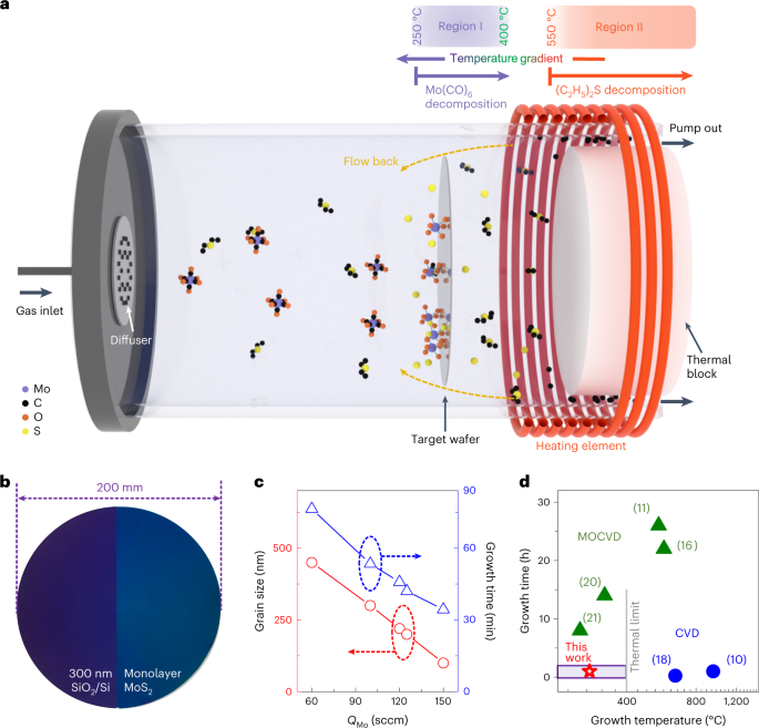
Kang, K. et al. High-mobility three-atom-thick semiconducting films with wafer-scale homogeneity. Nature 520, 656–660 (2015).
Yang, P. et al. Batch production of 6-inch uniform monolayer molybdenum disulfide catalyzed by sodium in glass. Nat. Commun. 9, 979 (2018).
Asselberghs, I. et al. Wafer-scale integration of double gated WS2-transistors in 300 mm Si CMOS fab. In Proc. 2020 IEEE International Electron Devices Meeting (IEDM) 40.2.1–40.2.4 (IEEE, 2020); https://doi.org/10.1109/IEDM13553.2020.9371926
O’Brien, K. P. et al. Advancing 2D monolayer CMOS through contact, channel and interface engineering. In Proc. 2021 IEEE International Electron Devices Meeting (IEDM) 7.1.1–7.1.4 (IEEE, 2021); https://doi.org/10.1109/IEDM19574.2021.9720651
Meng, W. et al. Three-dimensional monolithic micro-LED display driven by atomically thin transistor matrix. Nat. Nanotechnol. 16, 1231–1236 (2021).
Hwangbo, S. et al. Wafer-scale monolithic integration of full-colour micro-LED display using MoS2 transistor. Nat. Nanotechnol. 17, 500–506 (2022).
Koike, J., Hosseini, M., Hai, H. T., Ando, D. & Sutou, Y. Material innovation for MOL, BEOL, and 3D integration. In Proc. 2017 IEEE International Electron Devices Meeting (IEDM) 32.3.1–32.3.4 (IEEE, 2017); https://doi.org/10.1109/IEDM.2017.8268485
Zhang, W. et al. High-gain phototransistors based on a CVD MoS2 monolayer. Adv. Mater. 25, 3456–3461 (2013).
Yim, C. et al. High-performance hybrid electronic devices from layered PtSe2 films grown at low Temperature. ACS Nano 10, 9550–9558 (2016).
Park, J.-H. et al. Synthesis of high-performance monolayer molybdenum disulfide at low temperature. Small Methods 5, 2000720 (2021).
Mun, J. et al. High-mobility MoS2 directly grown on polymer substrate with kinetics-controlled metal–organic chemical vapor deposition. ACS Appl. Electron. Mater. 1, 608–616 (2019).
Schaefer, C. M. et al. Carbon Incorporation in MOCVD of MoS2 thin films grown from an organosulfide precursor. Chem. Mater. 33, 4474–4487 (2021).
Cole-Hamilton, D. J. & Williams, J. O. (eds) Mechanisms of Reactions of Organometallic Compounds with Surfaces (Plenum, 2014).
Nam, H. & Shin, C. Impact of current flow shape in tapered (versus rectangular) FinFET on threshold voltage variation induced by work-function variation. IEEE Trans. Electron. Devices 61, 2007–2011 (2014).
Zhang, C. et al. An accurate method to extract and separate interface and gate oxide traps by the MOSFET subthreshold current. In Technical Proc. 2011 NSTI Nanotechnology Conference and Expo Vol. 2 (eds Laudon, M. & Romanowicz, B.) 180–183 (Nano Science and Technology Institute, CRC, 2011).
Cheng, Z. et al. How to report and benchmark emerging field-effect transistors. Nat. Electron. 5, 416–423 (2022).
Bao, W. et al. High mobility ambipolar MoS2 field-effect transistors: substrate and dielectric effects. Appl. Phys. Lett. 102, 042104 (2013).
Illarionov, Y. Y. U. et al. Insulators for 2D nanoelectronics: the gap to bridge. Nat. Commun. 11, 3385 (2020).
Ma, N. & Jena, D. Charge scattering and mobility in atomically thin semiconductors. Phys. Rev. X 4, 011043 (2014).
Yu, Z. et al. Realization of room-temperature phonon-limited carrier transport in monolayer MoS2 by dielectric and carrier screening. Adv. Mater. 28, 547–552 (2016).
Liu, X. et al. A modified wrinkle-free MoS2 film transfer method for large area high mobility field-effect transistor. Nanotechnology 24, 055707 (2020).
Li, N. et al. Large-scale flexible and transparent electronics based on monolayer molybdenum disulfide field-effect transistors. Nat. Electron. 3, 177–717 (2020).
Sebastian, A. et al. Benchmarking monolayer MoS2 and WS2 field-effect transistors. Nat. Commun. 12, 693 (2021).
Seol, M. et al. High-throughput growth of wafer-scale monolayer transition metal dichalcogenide via vertical Ostwald ripening. Adv. Mater. 32, 2003542 (2020).
Kim, T. et al. Wafer-scale production of highly uniform two-dimensional MoS2 by metal–organic chemical vapor deposition. Nanotechnology 28, 18LT01 (2017).
Roy, A., Grossmann, P. J., Vitale, S. A. & Calhoun, B. H. A 1.3 µW, 5 pJ/cycle sub-threshold MSP430 processor in 90 nm xLP FDSOI for energy-efficient IoT applications. In Proc. 2016 17th International Symposium on Quality Electronic Design (ISQED) 158–162 (IEEE, 2016); https://doi.org/10.1109/ISQED.2016.7479193
Weller, H. G. et al. A tensorial approach to computational continuum mechanics using object-oriented techniques. Comput. Phys. 12, 620–631 (1998).
Peng, D.-Y. & Robinson, D. B. A new two-constant equation of state. Ind. Eng. Chem. Fundam. 15, 59–64 (1976).
Tkaczuk, J. et al. Equations of state for the thermodynamic properties of binary mixtures for helium-4, neon, and argon. J. Phys. Chem. Ref. Data 49, 023101 (2020).
Tegeler, C. et al. A new equation of state for argon covering the fluid region for temperatures from the melting line to 700 K at pressures up to 1000 MPa. J. Phys. Chem. Ref. Data 28, 779–850 (1999).
Lemmon, E. W. & Jacobsen, R. T. Viscosity and thermal conductivity equations for nitrogen, oxygen, argon, and air. Int. J. Thermophys. 25, 21–69 (2004).
Darwish, M. & Moukalled, F. The Finite Volume Method in Computational Fluid Dynamics: An Advanced Introduction with OpenFOAM® and Matlab® (Springer, 2021).
- SEO Powered Content & PR Distribution. Get Amplified Today.
- PlatoAiStream. Web3 Data Intelligence. Knowledge Amplified. Access Here.
- Minting the Future w Adryenn Ashley. Access Here.
- Source: https://www.nature.com/articles/s41565-023-01375-6
- ][p
- $UP
- 1
- 1.3
- 10
- 11
- 12
- 13
- 14
- 1998
- 1999
- 20
- 200
- 2011
- 2012
- 2014
- 2015
- 2016
- 2017
- 2018
- 2019
- 2020
- 2021
- 2022
- 22
- 23
- 24
- 26
- 27
- 28
- 2D
- 30
- 39
- 3d
- 7
- 8
- 9
- a
- accurate
- advanced
- AIR
- AL
- an
- and
- applications
- approach
- AREA
- article
- At
- based
- Benchmark
- BRIDGE
- built
- by
- carbon
- Channel
- charge
- chemical
- click
- complementary
- conductivity
- Conference
- contact
- Continuum
- could
- covering
- CRC
- Current
- Design
- Devices
- directly
- Display
- double
- driven
- dynamics
- e
- E&T
- effects
- Electronic
- Electronics
- emerging
- end
- energy
- Engineering
- equations
- Ether (ETH)
- extend
- extract
- Film
- films
- flexible
- flow
- fluid
- Fluid dynamics
- For
- from
- future
- gap
- gated
- glass
- Graphene
- grown
- Growth
- Harvesting
- High
- high-performance
- highly
- How
- How To
- http
- HTTPS
- Hybrid
- i
- IEEE
- Impact
- in
- Innovation
- Institute
- integrated
- integration
- Interface
- International
- Introduction
- iot
- large
- large-scale
- Law
- layer
- layered
- Line
- LINK
- Low
- material
- Matrix
- mechanics
- meeting
- metal
- method
- mobility
- Modern
- modified
- MOL
- Monolithic
- nano
- nanotechnology
- Nature
- Neon
- New
- of
- on
- Oxygen
- platform
- plato
- Plato Data Intelligence
- PlatoData
- policy
- polymer
- precursor
- PROC
- Processor
- Production
- properties
- quality
- reactions
- real-time
- realization
- region
- report
- research
- s
- Science
- Science and Technology
- screening
- semiconductor
- Semiconductors
- separate
- Shape
- Silicon
- single
- State
- Symposium
- techniques
- Technology
- The
- thermal
- three-dimensional
- threshold
- Through
- to
- transfer
- transition
- transparent
- transport
- traps
- using
- Versus
- via
- Voltage
- volume
- W
- Williams
- wireless
- with
- X
- zephyrnet

