Chiplets (die stacking) is not new. The origins are deeply rooted in the semiconductor industry and represent a modular approach to designing and manufacturing integrated circuits. The concept of chiplets has been energized as a response to the recent challenges posed by the increasing complexity of semiconductor design. Here are some well documented points about the demand for chiplets:
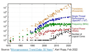
Complexity of Integrated Circuits (ICs): As semiconductor technology advanced, the complexity of designing and manufacturing large monolithic ICs increased. This led to challenges in terms of yield, cost, skilled resources, and time-to-market.
Moore’s Law: The semiconductor industry has been following Moore’s Law, which suggests that the number of transistors on a microchip doubles approximately every two years. This relentless scaling of transistor density poses challenges for traditional monolithic designs.
다양한 애플리케이션: Different applications require specialized components and features. Instead of creating a monolithic chip that tries to cater to all needs, chiplets allow for the creation of specialized components that can be combined in a mix-and-match fashion.
Cost and Time-to-Market Considerations: Developing a new semiconductor process technology is an expensive and time-consuming endeavor. Chiplets provide a way to leverage existing mature processes for certain components while focusing on innovation for specific functionalities. Chiplets also aid in the ramping of new process technologies since the die sizes and complexity are a fraction of a monolithic chip thus easing manufacturing and yield.
Interconnect Challenges: Traditional monolithic designs faced challenges in terms of interconnectivity as the distance between components increased. Chiplets allow for improved modularity and ease of interconnectivity.
Heterogeneous Integration: Chiplets enable the integration of different technologies, materials, and functionalities on a single package. This approach, known as heterogeneous integration, facilitates the combination of diverse components to achieve better overall performance.
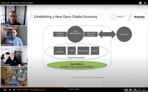
업계 협력: The development of chiplets often involves collaboration between different semiconductor companies and industry players. Standardization efforts, such as those led by organizations like the Universal Chiplet Interconnect Express Consortium (UCIe) for chiplet integration.
하단 라인 : Chiplets emerged as a solution to address the challenges posed by the increasing complexity, cost, time-to-market, and staffing pressures in the semiconductor industry. The modular and flexible nature of chiplet-based designs allows for more efficient and customizable integration of chips, contributing to advancements in semiconductor technology, not to mention the ability to multi source die.
인텔
Intel really has capitalized on chiplets which is key to their IDM 2.0 strategy.
There are two major points:
Intel will use chiplets to deliver 5 process nodes in 4 years which is a critical milestone in the IEDM 2.0 strategy (Intel 7, 4, 3, 20A, 18A).
Intel developed the Intel 4 process for internal products using chiplets. Intel developed CPU chiplets which is much easier to do than the historically monolithic CPU chips. Chiplets can be used to ramp a process much quicker and Intel can claim success without having to do a full process for complex CPUs or GPUs. Intel can then release a new process node (Intel 3) for foundry customers which can design monolithic or chiplet based chips. Intel is also doing this for 20A and 18A thus the 5 process nodes in 4 years milestone. This accomplishment is debatable of course but I see no reason to.
Intel will use chiplets in order to outsource manufacturing (TSMC) when business dictates.
Intel signed a historical outsourcing agreement with TSMC for chiplets. This is a clear proof of concept to get us back to the multi sourcing foundry business model that we enjoyed up until the FinFET era. I do not know if Intel will continue to use TSMC beyond the N3 node but the point has been made. We are no longer bound by a single source for chip manufacturing.
Intel can use this proof of concept (using chiplets from multiple foundries and packaging them up) for foundry business opportunities where customers want the freedom of multiple foundries. Intel is the first company to do this.
TSMC
There are two major points:
With chiplets TSMC avoids the M word (monopoly).
Using chiplets customers can theoretically multi source where their die comes from. Last I heard TSMC would not package die from other foundries but if a whale like Nvidia asked them to I’m sure they would.
Chiplets will challenge TSMC and TSMC is always up for a challenge because with challenge comes innovation.
TSMC quickly responded to chiplets with their 3D 패브릭 comprehensive family of 3D Silicon Stacking and Advanced Packaging Technologies. The greatest challenge for chiplets today is the supporting ecosystem and that is what TSMC is all about, ecosystem.
Back to the original question “How Disruptive will Chiplets be for Intel and TSMC?” Very much so. We are in the beginning of a semiconductor manufacturing disruption that we have not seen since FinFETs. All pure-play and IDM foundries now have the opportunity to get a piece of the chips that the world depends on, absolutely.
또한 읽기 :
2024년 빅 레이스는 TSMC N2와 Intel 18A
IEDM: What Comes After Silicon?
IEDM: TSMC Ongoing Research on a CFET Process
IEDM Buzz – Intel, 새로운 수직형 트랜지스터 스케일링 혁신 선보여
다음을 통해이 게시물 공유 :
- SEO 기반 콘텐츠 및 PR 배포. 오늘 증폭하십시오.
- PlatoData.Network 수직 생성 Ai. 자신에게 권한을 부여하십시오. 여기에서 액세스하십시오.
- PlatoAiStream. 웹3 인텔리전스. 지식 증폭. 여기에서 액세스하십시오.
- 플라톤ESG. 탄소, 클린테크, 에너지, 환경, 태양광, 폐기물 관리. 여기에서 액세스하십시오.
- PlatoHealth. 생명 공학 및 임상 시험 인텔리전스. 여기에서 액세스하십시오.
- 출처: https://semiwiki.com/chiplet/340742-how-disruptive-will-chiplets-be-for-intel-and-tsmc/
- :있다
- :이다
- :아니
- :어디
- $UP
- 3d
- 7
- a
- 능력
- 소개
- 절대적으로
- 달성
- 주소
- 많은
- 발전
- 후
- 협약
- 도움
- All
- 수
- 수
- 또한
- 항상
- an
- 및
- 어플리케이션
- 접근
- 대략
- 있군요
- AS
- 뒤로
- 기반으로
- BE
- 때문에
- 된
- 처음
- 더 나은
- 사이에
- 그 너머
- 큰
- 묶인
- 사업
- 비즈니스 모델
- 비자 면제 프로그램에 해당하는 국가의 시민권을 가지고 있지만
- by
- CAN
- 대문자
- 네 끗패
- 어떤
- 도전
- 과제
- 칩
- 칩
- 청구
- 선명한
- 협동
- 결합
- 결합 된
- 제공
- 기업
- 회사
- 복잡한
- 복잡성
- 구성 요소들
- 포괄적 인
- 개념
- 고려 사항
- 협회
- 계속
- 기여
- 비용
- 코스
- CPU
- 만들기
- 창조
- 임계
- 고객
- 맞춤형
- 깊이
- 배달하다
- 수요
- density
- 따라
- 디자인
- 설계
- 디자인
- 개발
- 개발
- 개발
- 지시하다
- Mourir
- 다른
- 붕괴
- disruptive
- 거리
- 몇몇의
- do
- 문서화 된
- 하기
- 더블스
- 완화
- 쉽게
- 편한
- 생태계
- 효율적인
- 노력
- 등장
- 가능
- 노력하다
- 대
- 모든
- 현존하는
- 비싼
- 급행
- 직면
- 을 용이하게
- 가족
- 패션
- 특징
- 먼저,
- 융통성있는
- 초점
- 수행원
- 럭셔리
- 주조
- 분수
- 자유
- 에
- 가득 찬
- 기능성
- 얻을
- GPU
- 가장 큰
- 있다
- 데
- 들었다
- 여기에서 지금 확인해 보세요.
- 역사적인
- 역사적으로
- 방법
- HTTPS
- i
- ICS
- if
- 개선하는
- in
- 증가
- 증가
- 산업
- 혁신
- 를 받아야 하는 미국 여행자
- 통합 된
- 완성
- 인텔
- 내부의
- 포함
- JPG
- 키
- 알아
- 알려진
- 넓은
- 성
- 법
- 지도
- 이점
- 처럼
- 라인
- 이상
- 만든
- 주요한
- 제조
- 재료
- 성숙한
- 최대 폭
- 언급
- 획기적 사건
- 모델
- 모듈러
- 단단히 짜여 하나로 되어 있는
- 배우기
- 보다 효율적으로
- 많은
- 멀티
- 여러
- 자연
- 요구
- 신제품
- 아니
- 노드
- 노드
- 지금
- 번호
- 엔비디아
- of
- 자주
- on
- 지속적으로
- 기회
- 기회
- or
- 주문
- 조직
- 실물
- 태생
- 기타
- 외주
- 아웃소싱
- 전체
- 꾸러미
- 포장
- 성능
- 조각
- 플라톤
- 플라톤 데이터 인텔리전스
- 플라토데이터
- 플레이어
- 포인트 적립
- 전철기
- 제기
- 포즈
- 게시하다
- 미리
- 방법
- 프로세스
- 제품
- 발기인
- 증명
- 개념 증명
- 제공
- 문제
- 빨리
- 빨리
- 경주
- 비탈길
- 램핑
- 읽기
- 정말
- 이유
- 최근
- 공개
- 잔인한
- 대표
- 필요
- 연구
- 제품 자료
- 응답
- 뿌리 박은
- 스케일링
- 참조
- 본
- 반도체
- 서명
- 규소
- 이후
- 단일
- 크기
- 숙련 된
- So
- 해결책
- 일부
- 출처
- 소싱
- 전문
- 구체적인
- 스태킹
- 직원
- 표준화
- 전략
- 성공
- 이러한
- 제안
- 지원
- 확인
- 기술
- Technology
- 조건
- 보다
- 그
- XNUMXD덴탈의
- 세계
- 그들의
- 그들
- 그때
- 그들
- 이
- 그
- 그러므로
- 시간이 많이 걸리는
- 에
- 오늘
- 전통적인
- 티엠씨
- 두
- 보편적 인
- 까지
- us
- 사용
- 익숙한
- 사용
- 수직선
- 대단히
- 를 통해
- 필요
- 방법..
- we
- 잘
- 고래
- 뭐
- 언제
- 어느
- 동안
- 의지
- 과
- 없이
- 워드
- 세계
- 겠지
- 년
- 수율
- 제퍼 넷