News: Microelectronics
24 Maggio 2023
Cambridge GaN Devices Ltd (CGD) — which was spun out of the University of Cambridge Department of Engineering’s Electrical Power and Energy Conversion group in 2016 and designs, develops and commercializes power transistors and ICs that use GaN-on-silicon substrates — has introduced a range of Application Interface Boards that allow designers to try out its ICeGaN high-electron-mobility transistors (HEMTs) in existing circuits in place of competing MOSFET or GaN devices without having to re-layout the PCB.
Application Interface Boards are adaptor PCBs that are soldered to an ICeGaN device, which map each pin/signal from the ICeGaN HEMT footprint to the corresponding pins/signals of an alternative component footprint.
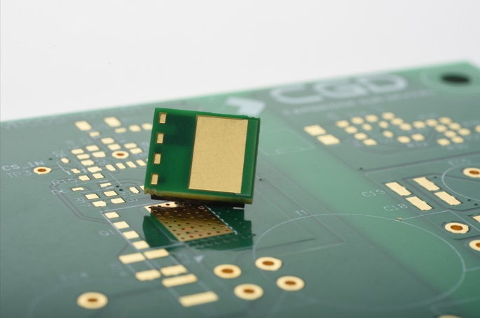
“These Application Interface Boards are designed for design and evaluation purposes only, of course. This is a quick, first step to enable the user to put one of our ICeGaN ICs into an existing design,” says Peter Comiskey, director of application engineering. “There is some minor impact on thermal performance, but surprisingly little difference in EMC or electrical performance.”
CGD offers Application Interface Boards for a number of industry-standard devices from leading MOSFET and GaN device makers. A full list can be found on the guida utente, but the firm can also develop an Application Interface Board for devices not currently supported for delivery within four weeks.
Gli HEMT ICeGaN di CGD sono disponibili in grandi volumi
- Distribuzione di contenuti basati su SEO e PR. Ricevi amplificazione oggi.
- PlatoAiStream. Intelligenza dei dati Web3. Conoscenza amplificata. Accedi qui.
- Coniare il futuro con Adryenn Ashley. Accedi qui.
- Acquista e vendi azioni in società PRE-IPO con PREIPO®. Accedi qui.
- Fonte: https://www.semiconductor-today.com/news_items/2023/may/cgd-240523.shtml
- :ha
- :È
- :non
- 2016
- a
- consentire
- anche
- alternativa
- an
- ed
- Applicazioni
- SONO
- disponibile
- BE
- tavola
- ma
- cambridge
- Materiale
- concorrenti
- componente
- Conversione
- Corrispondente
- corso
- Attualmente
- consegna
- Shirts Department
- Design
- progettato
- designer e gli illustratori veneziani,
- disegni
- sviluppare
- sviluppa
- dispositivo
- dispositivi
- differenza
- Direttore
- ogni
- enable
- energia
- Ingegneria
- valutazione
- esistente
- Impresa
- Nome
- Orma
- Nel
- essere trovato
- quattro
- da
- pieno
- Gruppo
- avendo
- Alta
- http
- HTTPS
- ICS
- Impact
- in
- Interfaccia
- ai miglioramenti
- introdotto
- Introduce
- elementi
- SUO
- jpg
- principale
- Lista
- piccolo
- Ltd
- Makers
- carta geografica
- Maggio..
- minore
- numero
- of
- Offerte
- on
- ONE
- esclusivamente
- or
- nostro
- su
- PCB
- performance
- Peter
- posto
- Platone
- Platone Data Intelligence
- PlatoneDati
- energia
- fini
- metti
- Presto
- gamma
- relazionato
- dice
- alcuni
- spun
- step
- supportato
- che
- I
- termico
- questo
- a
- prova
- Università
- Università di Cambridge
- uso
- Utente
- Prima
- Settimane
- quale
- entro
- senza
- zefiro