In a typical day in the life of a product engineer, they have gone through the requisite wafer sort testing in manufacturing with the next step to assemble the resultant good die into their respective packages. While performing a series of parametric tests during final test, yield issues are encountered and the process of finding the source of the issues begins. Luckily, with access to a good data analytics solution, it is possible to trace the life of the silicon back through previous high volume test manufacturing stages such as assembly, wafer sort, wafer acceptance testing as well as through the earlier NPI manufacturing stage where access to the design, diagnostics data as well as pre-silicon timing tools and post-silicon failure analysis (FA) tools are available.
Traceability of the failed packaged die back through earlier assembly, wafer sort and wafer acceptance test data reveal no correlation of why these die are now failing at final test. However, correlation with diagnostic data shows that the failing packaged die in final test were geospatially close to die on a wafer map that had failed specific scan tests during wafer sort. Furthermore, no FA was performed on those die that failed these specific scan tests as they were not considered one of the main systematic yield issues during In-Ramp. The diagnostic data did reveal, however, that the scan failures were likely due to a timing problem in several critical paths in the silicon since several transition delay fault (TDF) scan tests had failed.
One quick way to solve this timing issue is to go back to the pre-silicon timing models and derate all the cells while redoing synthesis and place and route to meet timing in the real silicon. However, this would result in using larger, faster cells in areas of the chip that were not needed and will use more overall power than before, causing battery life issues or potentially shortening the life of the device in use over time.
Instead of this approach, there is a better solution. First, the engineer can send the actual monitor and sensor data from early NPI test chips to the timing tool to have it recalibrate the timing models for enhanced accuracy; second, have it evaluate several failed paths from diagnostics to see if there are any cells in the paths in question that have timing issues. Hence, do any cells contain “negative” slack which would explain the failing scan tests? In this example, say one particular library cell out of all of the cells within several failed paths was found to generate significant delay, causing the timing issue. To confirm the findings, it is necessary to send several failed packaged die from final test along with the detailed diagnostic data to the FA tool for further electrical and physical FA analysis; here it can be uncovered that indeed this one cell was slow and thus, the cause of the timing failure in the actual silicon.
The reason that more parts fail during final test than in scan tests during wafer sort is because they are tested under different environmental conditions. Further analysis, such as automated Vmin estimation, shows the required voltage these die would need to operate at to pass. In this example, perhaps the minimum operating voltage that would allow the parts to pass exceeds the power/performance profile requirement of this chip’s specification. Thus, the need for a design change.
The design change in this example entails the derating of only this one slow library cell such that a different yet possibly faster and larger cell will be selected in its place during the synthesis, place and route. The foundry would also be notified of the original slow, inaccurate cell model. While the new cell selected will generate more power which is necessary for specific devices, it may be possible to identify other cells that can be downgraded to slower, smaller cells to compensate for the additional power attributed by the new cell. Hence, the same overall power and performance profile is preserved.
This is just one example that product engineers could experience frequently. Without access to an appropriate analytics solution that supports out-of-the-box insights, die-to-die traceability and correlation of many data types across all phases of the lifecycle, this particular problem may have taken months instead of days or weeks to find and correct. The end result unfortunately could be potential lost revenue as well as higher manufacturing costs due to scrapping unexpected failed devices and expensive packaging. In addition, there could be recurring costs associated with extensive tester time.
Synopsys SLM
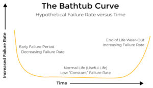
The industry vision for Silicon Lifecycle Management (SLM) is to provide the ability to monitor the health of silicon throughout its life from early design through manufacturing and then onto in-field while the silicon is in use, as shown in figure 1 below. However, it not only can monitor the health of silicon devices but also have a direct positive impact on it by optimizing the chip’s operational metrics such as power and performance. In addition, being able to quickly perform root cause analysis to debug any significant yield or quality issues at any given point in the silicon’s journey is also paramount.

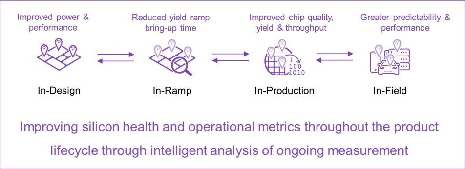
Fig. 1: Synopsys SLM – Lifecycle Phases
However, monitoring, optimizing and debugging across the entire life of the silicon is no trivial task on today’s advanced chips, SoCs and MDSs (multi-die systems), which continue to grow significantly in scale and complexity. There are also complexities of the design, manufacturing and test processes including many different data types to support which further complicate this challenge.
The solution centers around the data captured from silicon with the ability to perform the following requirements:
- Add visibility within the silicon with the use of monitors and sensors to monitor what’s really going on during the operation of the chip or device
- Consume and analyze extremely large amounts of data
- Provide actionable insights to direct the engineer as to where their issues reside or identify key points of interest
These requirements are all top-of-mind within fabless and IDM companies today. Figure 2 below shows the procedural steps associated with the lifecycle phases that need to be implemented to allow for monitoring, optimizing and debugging of the silicon throughout its life.
- Step 1: In-chip monitors such as power, voltage and temperature or newer advanced path margin monitors are inserted into the design to later monitor the operational attributes of the silicon during operation in each phase of its life.
- Step 2: All relevant test and design data are stored and made available for analysis. However, traditional test manufacturing data such as wafer acceptance test (WAT), bump, wafer sort (WS), assembly, final test (FT) and system-level test (SLT) is no longer sufficient to provide root cause analysis of issues. Data from the monitors and sensors, design data (LEF/DEF/GDS), fab data if available (in-line metrology, defectivity) and diagnostic data (from scan ATPG or memory BIST patterns) are needed.
- Step 3: Perform analysis based on customized analytics for the given lifecycle phase. The analytics engine provides actionable insights with die-level traceability enabled throughout the manufacturing process with single click correlation capabilities across all data types to pinpoint issues automatically within seconds. It should be common to perform root cause analysis of most issues within a matter of several directed clicks into various provided drilldown views of your data.
- Step 4: Act on the issue by performing corrective action or specific production control measures no matter where the silicon resides within the lifecycle process. For example, corrective action for In-Design could be to analyze the silicon data from the embedded monitors early during the NPI ramp stage and compare these actual results against the pre-silicon timing models for opportunities to perform design margin optimization to further reduce the power of your chip while still maintaining the operating performance (frequency, voltage).

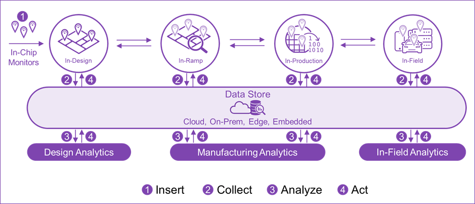
Fig. 2: Synopsys SLM – Executable Steps
The power (and need) for unification
Each individual phase of the silicon lifecycle has its own unique challenges whether it be over design margining in-design, systematic yield ramp issues in-ramp, quality excursions and new-found yield issues in-production or maintainability and reliability in-field. Each of these challenges has a solution to address each of them individually. However, unless these challenges are caught during their respective phase in the lifecycle, they are increasingly difficult to identify and isolate as the design progresses down that lifecycle phases.
As explained in the earlier example, having to traverse back through the different lifecycle phases to identify the root cause is no trivial feat. It requires die-to-die level traceability and automated correlation capabilities correlating against many different data types as mentioned. Therefore, for complex advanced node designs, having an integrated solution that unifies various phases of the silicon lifecycle is becoming crucial to quickly identify root cause and minimize the effects of these issues which may manifest in profound consequences such as lost product revenue, increased manufacturing costs or raised public safety concerns.
Synopsys has invested in addressing these major concerns by creating a new SLM analytics solution that combines the design and product manufacturing phases into a single complete homogeneous platform, as shown below in figure 3.


Fig. 3: Integrated SLM analytics solution from design through manufacturing.
The benefits of having such a unified solution can be realized in the following three key focus areas: Productivity, Efficiency and Scalability.
Productivity
Most data today are either unused by engineers due to the massive amount or lack of automation on where to look for issues within this data. With this solution, engineers are now able to gain instant value from all data integrated into one solution. Automated analysis and identification of issues are displayed in the form of insights. Part-level traceability and debug enables quick root cause analysis along with corrective action back into the supply chain. Sub-die analysis is also available in early NPI product stage to identify systematic issues for further failure analysis that are preventing high yield and prohibiting the move to high-volume production.
Efficiency
Chip power and performance optimization is made possible by the inclusion of monitors into the design, enabling feedback of the monitor data for performing design calibration. An automated recipe flow for quality optimization containing outlier detection techniques is provided during production control back into the manufacturing supply chain. Comprehensive yield optimization is enabled by combining yield trend analysis, diagnostics and failure analysis with improvements made back into the design and/or process. OEE (overall equipment effectiveness) analysis of the tester fleet enables throughput optimization of the chip production. Real-time data collection and production control at the ATE test cell is provided for fast latency of correcting issues resulting in improved test cost savings and quality escape prevention.
Scalability
The enhanced product architecture of this solution accommodates petabytes of data across the full breadth of data types including design, monitor, diagnostic, fab and production test, which most analytics tools cannot process either this breadth or depth of data. Having a solution able to handle massive amounts of data becomes crucial for performing timely root cause analysis, especially when debugging silicon chip issues further downstream in manufacturing, debugging RMAs (return merchandise authorization) or performing historical analysis. Also, having the flexibility to provide users with an option for processing and storing their data on the cloud is critical.
For more information on SLM and this new unified solution, please visit us at Silicon Lifecycle Management Platform (synopsys.com) or email us at [email protected].

Guy Cortez
(all posts)Guy Cortez is a staff product marketing manager for silicon lifecycle management in Synopsys' Digital Design Group. His marketing career spans more than 20 years. He has held various marketing positions, including technical, product/solution, channel/field, integrated/corporate, alliance and business development for companies such as Synopsys, Cadence, VMware and Optimal+. Prior to that, Cortez spent 12 years as a test engineer at Hughes Aircraft Company (now Boeing), and later at Sunrise Test Systems (which became Viewlogic, and later Synopsys). At Hughes, he was responsible for generating all of the manufacturing test programs for the ASICs developed in the Missile Systems Group Division. At Sunrise, Cortez was a pre and post-sales applications engineer, and also doubled as the company’s instructor.
- SEO Powered Content & PR Distribution. Get Amplified Today.
- PlatoAiStream. Web3 Data Intelligence. Knowledge Amplified. Access Here.
- Minting the Future w Adryenn Ashley. Access Here.
- Source: https://semiengineering.com/silicon-lifecycle-management-advances-with-unified-analytics/
- :has
- :is
- :not
- :where
- 1
- 20
- 20 years
- 22
- 320
- a
- ability
- Able
- acceptance
- access
- accuracy
- across
- Act
- Action
- addition
- Additional
- address
- addressing
- advanced
- advances
- against
- aircraft
- All
- All Posts
- Alliance
- along
- also
- amount
- amounts
- an
- analysis
- analytics
- analyze
- and
- any
- applications
- approach
- appropriate
- architecture
- ARE
- areas
- around
- AS
- Asics
- Assembly
- associated
- At
- attributes
- authorization
- Automated
- automatically
- Automation
- available
- back
- based
- battery
- Battery life
- BE
- became
- because
- becomes
- becoming
- before
- being
- below
- benefits
- Better
- Boeing
- breadth
- business
- business development
- but
- by
- Cadence
- CAN
- cannot
- capabilities
- Career
- caught
- Cause
- causing
- Cells
- Centers
- chain
- challenge
- challenges
- change
- chip
- Chips
- click
- Close
- Cloud
- collection
- COM
- combines
- combining
- Common
- Companies
- company
- Company’s
- compare
- complete
- complex
- complexities
- complexity
- comprehensive
- Concerns
- conditions
- Confirm
- Consequences
- considered
- continue
- control
- correlating
- Correlation
- Cost
- cost savings
- Costs
- could
- Creating
- critical
- crucial
- customized
- data
- Data Analytics
- day
- Days
- delay
- depth
- Design
- designs
- detailed
- Detection
- developed
- Development
- device
- Devices
- DID
- Die
- different
- difficult
- digital
- direct
- Division
- do
- doubled
- down
- Downgraded
- during
- each
- Earlier
- Early
- effectiveness
- effects
- efficiency
- either
- embedded
- enabled
- enables
- enabling
- Engine
- engineer
- Engineers
- enhanced
- Entire
- environmental
- equipment
- especially
- evaluate
- example
- exceeds
- expensive
- experience
- Explain
- explained
- extensive
- extremely
- FAIL
- Failed
- Failure
- FAST
- faster
- feat
- feedback
- Figure
- final
- Find
- finding
- First
- FLEET
- Flexibility
- flow
- Focus
- following
- For
- form
- found
- Foundry
- Frequency
- frequently
- from
- FT
- full
- further
- Furthermore
- Gain
- generate
- generating
- given
- Go
- going
- good
- Group
- Grow
- Guy
- handle
- Have
- having
- he
- Health
- Held
- here
- High
- High Yield
- higher
- historical
- However
- HTML
- HTTPS
- Identification
- identify
- Impact
- implemented
- improved
- improvements
- in
- inaccurate
- Including
- inclusion
- increased
- increasingly
- individual
- Individually
- industry
- information
- insights
- instant
- instead
- integrated
- into
- invested
- issue
- issues
- IT
- ITS
- journey
- jpg
- just
- just one
- Key
- Lack
- large
- larger
- Latency
- Level
- Library
- Life
- lifecycle
- likely
- longer
- Look
- made
- Main
- major
- management
- manager
- manufacturing
- many
- map
- Margin
- Marketing
- massive
- Matter
- max-width
- May..
- measures
- Meet
- Memory
- mentioned
- merchandise
- Metrics
- Metrology
- minimum
- model
- models
- Monitor
- monitoring
- monitors
- months
- more
- most
- move
- necessary
- Need
- needed
- New
- next
- node
- now
- of
- on
- ONE
- only
- operate
- operating
- operation
- operational
- opportunities
- optimization
- optimizing
- Option
- or
- original
- Other
- over
- overall
- own
- packages
- packaging
- Paramount
- particular
- parts
- pass
- path
- patterns
- perform
- performance
- performing
- perhaps
- phase
- physical
- Place
- platform
- plato
- Plato Data Intelligence
- PlatoData
- please
- Point
- points
- positions
- positive
- possible
- possibly
- Posts
- potential
- potentially
- power
- pre
- preventing
- Prevention
- previous
- Prior
- Problem
- process
- processes
- processing
- Product
- Production
- productivity
- Profile
- profound
- Programs
- protected
- provide
- provided
- provides
- public
- quality
- question
- Quick
- quickly
- raised
- Ramp
- real
- real-time
- real-time data
- realized
- really
- reason
- recipe
- recurring
- reduce
- relevant
- reliability
- required
- requirement
- Requirements
- requires
- requisite
- respective
- responsible
- result
- resulting
- Results
- return
- reveal
- revenue
- root
- Route
- Safety
- same
- Savings
- Scalability
- Scale
- scan
- Second
- seconds
- see
- selected
- sensors
- Series
- several
- should
- shown
- Shows
- significant
- significantly
- Silicon
- since
- single
- slack
- slow
- smaller
- solution
- SOLVE
- Source
- spans
- specific
- specification
- spent
- Staff
- Stage
- stages
- Step
- Steps
- Still
- stored
- such
- sufficient
- supply
- supply chain
- support
- Supports
- Systems
- Task
- Technical
- techniques
- test
- Testing
- tests
- than
- that
- The
- The Source
- their
- Them
- There.
- therefore
- These
- they
- this
- those
- three
- Through
- throughout
- throughput
- thumbnail
- time
- timing
- to
- today
- today’s
- tool
- tools
- trace
- Traceability
- traditional
- transition
- Trend
- trend analysis
- types
- typical
- under
- Unexpected
- unfortunately
- unified
- unique
- unused
- us
- use
- users
- using
- value
- various
- views
- visibility
- vision
- Visit
- vmware
- Voltage
- volume
- was
- Way..
- Weeks
- WELL
- were
- when
- whether
- which
- while
- why
- will
- with
- within
- without
- would
- years
- Yield
- Your
- zephyrnet