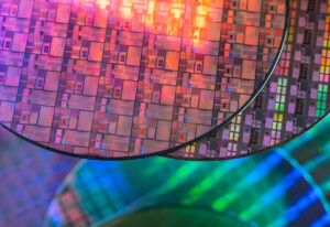
Lithographers have always faced tradeoffs between speed and flexibility. Steppers are very good at printing hundreds or thousands of identical features onto hundreds or thousands of wafers. They are not especially good at handling surfaces with significant topography, though. Nor is customization feasible. Every exposure uses the same reticle.
Direct write e-beam lithography has long been used by photomask shops, where it is justified by the need for near-perfection in high-precision “tooling.” The advantages of maskless lithography are less clear elsewhere in the process. Direct laser imaging dissipates a lot of heat into the photoresist, and resolution is limited by the dimensions of the laser spot. Most direct-write tools are slow compared to comparable steppers.
At the same time, advanced packaging and MEMS applications are very challenging for conventional steppers. The topography of the surface being patterned can be uneven, especially in fan-out wafer level packaging. The desired features themselves are often quite thick, requiring thick photoresists.
Meanwhile, automotive applications in particular require individual part traceability for regulatory and security reasons. The ease of customization in maskless exposures makes them particularly well-suited to high security applications. A simple change in the last metal layer can be used to embed a chip’s serial number directly in the chip itself, before packaging and molding. Top-level wiring changes can be used to embed encryption keys, as well.
Maskless exposure system supports this kind of customization. More generally, though, it can be used to solve exposure problems that steppers can’t. For example, it can pattern arbitrary wafer-scale black resist shapes for CMOS image sensor lens shields and display applications, and with laser diodes at different wavelengths, it can expose two different photoresists in a single imaging pass.
Steppers aren’t going anywhere, of course. They are unsurpassed in situations calling for large numbers of identical features. When the features to be printed are not identical, though, or where the pattern is larger than a single mask, maskless lithography can fill the void.

Katherine Derbyshire
(all posts)
Katherine Derbyshire is a technical editor at Semiconductor Engineering.
- SEO Powered Content & PR Distribution. Get Amplified Today.
- PlatoData.Network Vertical Generative Ai. Empower Yourself. Access Here.
- PlatoAiStream. Web3 Intelligence. Knowledge Amplified. Access Here.
- PlatoESG. Automotive / EVs, Carbon, CleanTech, Energy, Environment, Solar, Waste Management. Access Here.
- PlatoHealth. Biotech and Clinical Trials Intelligence. Access Here.
- ChartPrime. Elevate your Trading Game with ChartPrime. Access Here.
- BlockOffsets. Modernizing Environmental Offset Ownership. Access Here.
- Source: https://semiengineering.com/is-maskless-lithography-coming-into-its-own/
- :has
- :is
- :not
- :where
- 27
- 60
- 80
- a
- advanced
- advantages
- All
- All Posts
- always
- and
- anywhere
- applications
- ARE
- AS
- At
- automotive
- BE
- been
- before
- being
- between
- Black
- by
- calling
- CAN
- challenging
- change
- Changes
- chip
- clear
- coming
- comparable
- compared
- conventional
- course
- customization
- desired
- different
- dimensions
- direct
- directly
- Display
- ease
- editor
- elsewhere
- embed
- encryption
- Engineering
- especially
- Every
- example
- Exposure
- faced
- feasible
- Features
- fill
- Flexibility
- For
- generally
- going
- good
- Handling
- Have
- High
- HTTPS
- Hundreds
- identical
- image
- Imaging
- in
- individual
- into
- IT
- ITS
- itself
- jpg
- keys
- Kind
- large
- larger
- laser
- Last
- layer
- Lens
- less
- Level
- Limited
- Long
- Lot
- MAKES
- mask
- metal
- more
- most
- Need
- nor
- number
- numbers
- of
- often
- or
- own
- packaging
- part
- particular
- particularly
- pass
- Pattern
- photo
- plato
- Plato Data Intelligence
- PlatoData
- Posts
- printing
- problems
- process
- reasons
- regulatory
- require
- Resolution
- same
- security
- semiconductor
- serial
- shapes
- shops
- significant
- Simple
- single
- situations
- slow
- SOLVE
- speed
- Spot
- Supports
- Surface
- system
- Technical
- than
- that
- The
- Them
- themselves
- they
- this
- though?
- thousands
- thumbnail
- time
- to
- tools
- top-level
- Traceability
- two
- used
- uses
- very
- wavelengths
- WELL
- when
- with
- write
- zephyrnet


