ม.ค. 24, 2024
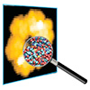
(ข่าวนาโนเวิร์ค) Researchers with the Department of Energy’s SLAC National Accelerator Laboratory, Stanford University and the DOE’s Lawrence Berkeley National Laboratory (LBNL) grew a twisted multilayer crystal structure for the first time and measured the structure’s key properties. The twisted structure could help researchers develop next-generation materials for solar cells, quantum computers, lasers and other devices.
“This structure is something that we have not seen before – it was a huge surprise to me,” said Yi Cui, a professor at Stanford and SLAC and paper co-author. “A new quantum electronic property could appear within this three-layer twisted structure in future experiments.”
 แคปชั่น
เพิ่มชั้นด้วยการบิด
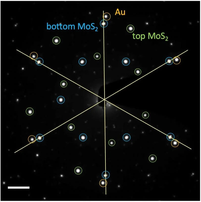
The crystals the team designed extended the concept of epitaxy, a phenomenon that occurs when one type of crystal material grows on top of another material in an ordered way – kind of like growing a neat lawn on top of soil, but at the atomic level. Understanding epitaxial growth has been critical to the development of many industries for more than 50 years, particularly the semiconductor industry. Indeed, epitaxy is part of many of the electronic devices that we use today, from cell phones to computers to solar panels, allowing electricity to flow, and not flow, through them. To date, epitaxy research has focused on growing one layer of material onto another, and the two materials have the same crystal orientation at the interface. This approach has been successful for decades in many applications, such as transistors, light-emitting diodes, lasers and quantum devices. But to find new materials that perform even better for more demanding needs, like quantum computing, researchers are searching for other epitaxial designs – ones that might be more complex, yet better performing, hence the “twisted epitaxy” concept demonstrated in this study. In their experiment, detailed in วิทยาศาสตร์ (“Twisted epitaxy of gold nanodisks grown between twisted substrate layers of molybdenum disulfide”) นักวิจัยได้เพิ่มชั้นทองคำระหว่างแผ่นวัสดุเซมิคอนดักเตอร์แบบดั้งเดิมสองแผ่น โมลิบดีนัมไดซัลไฟด์ (MoS)2). Because the top and bottom sheets were oriented differently, the gold atoms could not align with both simultaneously, which allowed the Au structure to twist, said Yi Cui, Professor Cui’s graduate student in materials science and engineering at Stanford and co-author of the paper. “With only a bottom MoS2 ทองคำก็ยินดีที่จัดให้อยู่ในแนวเดียวกัน จึงไม่เกิดการบิดเบี้ยว” Cui นักศึกษาระดับบัณฑิตศึกษากล่าว “แต่ด้วย MoS ที่บิดเบี้ยวสองตัว2 แผ่นทองไม่แน่ใจว่าจะตรงกับชั้นบนหรือล่าง เราสามารถช่วยทองคำแก้ปัญหาความสับสน และค้นพบความสัมพันธ์ระหว่างการวางแนวของ Au และมุมบิดของ MoS สองชั้น2".การดูดซับแผ่นนาโนทองคำ
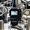
เพื่อศึกษาชั้นทองคำอย่างละเอียด ทีมนักวิจัยจากสถาบันวิทยาศาสตร์วัสดุและพลังงานสแตนฟอร์ด (SIMES) และ LBNL ได้อุ่นตัวอย่างโครงสร้างทั้งหมดที่อุณหภูมิ 500 องศาเซลเซียส จากนั้นพวกเขาก็ส่งกระแสอิเล็กตรอนผ่านตัวอย่างโดยใช้เทคนิคที่เรียกว่ากล้องจุลทรรศน์อิเล็กตรอนแบบส่องผ่าน (TEM) ซึ่งเผยให้เห็นลักษณะทางสัณฐานวิทยา การวางแนว และความเครียดของแผ่นนาโนทองคำหลังจากการหลอมที่อุณหภูมิต่างๆ การวัดคุณสมบัติเหล่านี้ของแผ่นนาโนทองคำเป็นขั้นตอนแรกที่จำเป็นในการทำความเข้าใจว่าโครงสร้างใหม่นี้สามารถออกแบบสำหรับการใช้งานในโลกแห่งความเป็นจริงได้อย่างไรในอนาคต “หากไม่มีการศึกษานี้ เราจะไม่รู้ว่าการบิดชั้นโลหะเหนือเซมิคอนดักเตอร์จะเป็นไปได้หรือไม่” Cui นักศึกษาระดับบัณฑิตศึกษากล่าว “การวัดโครงสร้างสามชั้นที่สมบูรณ์ด้วยกล้องจุลทรรศน์อิเล็กตรอนยืนยันว่าไม่เพียงแต่เป็นไปได้เท่านั้น แต่ยังสามารถควบคุมโครงสร้างใหม่ด้วยวิธีที่น่าตื่นเต้นอีกด้วย” ต่อไป นักวิจัยต้องการศึกษาเพิ่มเติมเกี่ยวกับคุณสมบัติทางแสงของแผ่นนาโนทองคำโดยใช้ TEM และเรียนรู้ว่าการออกแบบของพวกเขาเปลี่ยนแปลงคุณสมบัติทางกายภาพ เช่น โครงสร้างแถบของ Au หรือไม่ พวกเขายังต้องการขยายแนวคิดนี้เพื่อพยายามสร้างโครงสร้างสามชั้นด้วยวัสดุเซมิคอนดักเตอร์และโลหะอื่นๆ Bob Sinclair ศาสตราจารย์ Charles M. Pigott จากโรงเรียนวัสดุศาสตร์และวิศวกรรมศาสตร์ของ Stanford และผู้ร่วมเขียนรายงานกล่าวว่า "เรากำลังเริ่มสำรวจว่าการรวมกันของวัสดุเหล่านี้เท่านั้นที่เอื้อให้เกิดสิ่งนี้ หรือเกิดขึ้นได้ในวงกว้างมากขึ้น" “การค้นพบนี้ถือเป็นการเปิดการทดลองชุดใหม่ทั้งหมดที่เราสามารถลองได้ เราอาจกำลังค้นหาคุณสมบัติของวัสดุใหม่ที่เราสามารถนำมาใช้ประโยชน์ได้”- เนื้อหาที่ขับเคลื่อนด้วย SEO และการเผยแพร่ประชาสัมพันธ์ รับการขยายวันนี้
- PlatoData.Network Vertical Generative Ai เพิ่มพลังให้กับตัวเอง เข้าถึงได้ที่นี่.
- เพลโตไอสตรีม. Web3 อัจฉริยะ ขยายความรู้ เข้าถึงได้ที่นี่.
- เพลโตESG. คาร์บอน, คลีนเทค, พลังงาน, สิ่งแวดล้อม แสงอาทิตย์, การจัดการของเสีย. เข้าถึงได้ที่นี่.
- เพลโตสุขภาพ เทคโนโลยีชีวภาพและข่าวกรองการทดลองทางคลินิก เข้าถึงได้ที่นี่.
- ที่มา: https://www.nanowerk.com/nanotechnology-news3/newsid=64500.php
- :มี
- :เป็น
- :ไม่
- 10
- 13
- 14
- 24
- 50
- 50 ปี
- 500
- 7
- 8
- 9
- a
- คันเร่ง
- เพิ่ม
- ที่เพิ่ม
- หลังจาก
- จัดแนว
- อนุญาตให้
- การอนุญาต
- ช่วยให้
- ด้วย
- an
- และ
- อื่น
- ปรากฏ
- การใช้งาน
- เข้าใกล้
- เป็น
- AS
- At
- อะตอม
- วงดนตรี
- BE
- เพราะ
- รับ
- ก่อน
- การเริ่มต้น
- เบิร์กลีย์
- ดีกว่า
- ระหว่าง
- เมล็ดข้าว
- ทั้งสอง
- ด้านล่าง
- ยี่ห้อ
- แบรนด์นิว
- แต้
- สร้าง
- แต่
- ที่เรียกว่า
- CAN
- เซลล์
- โทรศัพท์มือถือ
- เซลล์
- เซลเซียส
- ศูนย์
- Charles
- ผู้เขียนร่วม
- การผสมผสาน
- สมบูรณ์
- ซับซ้อน
- คอมพิวเตอร์
- การคำนวณ
- แนวคิด
- ยืนยัน
- ความสับสน
- การควบคุม
- ได้
- วิกฤติ
- คริสตัล
- วันที่
- ทศวรรษที่ผ่านมา
- เรียกร้อง
- แสดงให้เห็นถึง
- แผนก
- ออกแบบ
- ได้รับการออกแบบ
- การออกแบบ
- รายละเอียด
- รายละเอียด
- พัฒนา
- พัฒนาการ
- อุปกรณ์
- ต่าง
- ต่างกัน
- ค้นพบ
- การค้นพบ
- DOE
- กระแสไฟฟ้า
- อิเล็กทรอนิกส์
- อิเล็กตรอน
- พลังงาน
- ชั้นเยี่ยม
- แม้
- น่าตื่นเต้น
- การทดลอง
- การทดลอง
- เอาเปรียบ
- สำรวจ
- ขยายออก
- ขยาย
- หา
- หา
- ชื่อจริง
- ครั้งแรก
- ไหล
- มุ่งเน้น
- สำหรับ
- ราคาเริ่มต้นที่
- ต่อไป
- อนาคต
- ทองคำ
- สำเร็จการศึกษา
- เพิ่มขึ้น
- การเจริญเติบโต
- เจริญเติบโต
- เติบโต
- การเจริญเติบโต
- ที่เกิดขึ้น
- มีความสุข
- มี
- ช่วย
- ด้วยเหตุนี้
- สรุป ความน่าเชื่อถือของ Olymp Trade?
- HTTPS
- ใหญ่
- if
- ภาพ
- in
- อุตสาหกรรม
- อุตสาหกรรม
- สถาบัน
- อินเตอร์เฟซ
- IT
- ITS
- jpg
- คีย์
- ชนิด
- ทราบ
- ห้องปฏิบัติการ
- เลเซอร์
- อเรนซ์
- ชั้น
- ชั้น
- เรียนรู้
- ชั้น
- กดไลก์
- การจัดการ
- หลาย
- วัสดุ
- การออกแบบวัสดุ
- วัสดุ
- me
- วัด
- การวัด
- โลหะ
- โลหะมีค่า
- กล้องจุลทรรศน์
- กลาง
- อาจ
- ข้อมูลเพิ่มเติม
- แห่งชาติ
- เรียบร้อย
- จำเป็น
- ความต้องการ
- ใหม่
- ถัดไป
- รุ่นต่อไป
- ไม่
- of
- on
- ONE
- คน
- เพียง
- การเปิด
- or
- อื่นๆ
- ของเรา
- แผง
- กระดาษ
- ส่วนหนึ่ง
- โดยเฉพาะ
- ดำเนินการ
- ที่มีประสิทธิภาพ
- ปรากฏการณ์
- โทรศัพท์
- กายภาพ
- เพลโต
- เพลโตดาต้าอินเทลลิเจนซ์
- เพลโตดาต้า
- เป็นไปได้
- ศาสตราจารย์
- คุณสมบัติ
- คุณสมบัติ
- ควอนตัม
- คอมพิวเตอร์ควอนตัม
- การคำนวณควอนตัม
- จริง
- โลกแห่งความจริง
- ความสัมพันธ์
- การวิจัย
- นักวิจัย
- นักวิจัย
- เปิดเผย
- s
- กล่าวว่า
- เดียวกัน
- โรงเรียน
- วิทยาศาสตร์
- วิทยาศาสตร์
- ค้นหา
- เห็น
- สารกึ่งตัวนำ
- ส่ง
- ชุด
- แผ่น
- พร้อมกัน
- So
- ดิน
- โซลา
- พลังงานแสงอาทิตย์
- แผงเซลล์แสงอาทิตย์
- แก้
- บางสิ่งบางอย่าง
- Stanford
- มหาวิทยาลัยสแตนฟอร์ด
- ขั้นตอน
- กระแส
- โครงสร้าง
- โครงสร้าง
- นักเรียน
- ศึกษา
- ที่ประสบความสำเร็จ
- อย่างเช่น
- แน่ใจ
- แปลกใจ
- ทีม
- เทคนิค
- ข้อความ
- กว่า
- ที่
- พื้นที่
- ก้าวสู่อนาคต
- ของพวกเขา
- พวกเขา
- แล้วก็
- ล้อยางขัดเหล่านี้ติดตั้งบนแกน XNUMX (มม.) ผลิตภัณฑ์นี้ถูกผลิตในหลายรูปทรง และหลากหลายเบอร์ความแน่นหนาของปริมาณอนุภาคขัดของมัน จะทำให้ท่านได้รับประสิทธิภาพสูงในการขัดและการใช้งานที่ยาวนาน
- พวกเขา
- นี้
- ตลอด
- เวลา
- ไปยัง
- ในวันนี้
- ด้านบน
- ไปทาง
- แบบดั้งเดิม
- ลอง
- บิด
- สอง
- ชนิด
- ความเข้าใจ
- มหาวิทยาลัย
- ใช้
- การใช้
- ต้องการ
- คือ
- ทาง..
- วิธี
- we
- คือ
- เมื่อ
- ว่า
- ที่
- ทั้งหมด
- กับ
- ภายใน
- โลก
- จะ
- ปี
- ยัง
- ลมทะเล
เพิ่มเติมจาก นาโนเวิร์ค
นักวิจัยแสดงให้เห็นว่าสิ่งกีดขวางควอนตัมและโทโพโลยีมีการเชื่อมโยงกันอย่างแยกไม่ออก
โหนดต้นทาง: 3057881
ประทับเวลา: ม.ค. 12, 2024
ภาพรวมแบบเรียลไทม์ครั้งแรกเกี่ยวกับพฤติกรรมการเติบโตของอนุภาคนาโน (พร้อมวิดีโอ)
โหนดต้นทาง: 2561111
ประทับเวลา: Mar 30, 2023

วิธีมองเห็นสิ่งที่มองไม่เห็น: ใช้การกระจายตัวของสสารมืดเพื่อทดสอบแบบจำลองจักรวาลวิทยาของเรา
โหนดต้นทาง: 2573474
ประทับเวลา: เมษายน 8, 2023
เร่งเซมิคอนดักเตอร์ที่ยั่งยืนด้วย 'หมึกหลายองค์ประกอบ'
โหนดต้นทาง: 2911790
ประทับเวลา: กันยายน 28, 2023
การออกแบบแม่เหล็กนาโนระดับโมเลกุลที่ขับเคลื่อนด้วยข้อมูล
โหนดต้นทาง: 1788884
ประทับเวลา: ธันวาคม 27, 2022
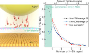
ขยายขีดจำกัดการเพิ่มประสิทธิภาพของพลาสโมนิคด้วยโบรอนไนไตรด์หกเหลี่ยม
โหนดต้นทาง: 2606223
ประทับเวลา: เมษายน 24, 2023

หนึ่งในสามของดาวเคราะห์ที่พบมากที่สุดในกาแล็กซีอาจอยู่ในเขตเอื้ออาศัยได้
โหนดต้นทาง: 2704960
ประทับเวลา: มิถุนายน 6, 2023
นาฬิกาจับเวลาแบบโอเพ่นซอร์สเพื่อจับเวลากิจกรรมระหว่างโมเลกุลภายในเซลล์ที่มีชีวิต
โหนดต้นทาง: 1921283
ประทับเวลา: ม.ค. 26, 2023
โพลีเมอร์ชนิดรีไซเคิลได้ที่สามารถรักษาได้ใหม่ช่วยให้หุ่นยนต์แบบอ่อนมีความสามารถในการปรับตัวสูง
โหนดต้นทาง: 2803734
ประทับเวลา: สิงหาคม 4, 2023