
Researchers have confined light to dimensions smaller than the diffraction limit in a nanosized dielectric cavity for the first time. The work, which confirms a theoretical prediction made in 2006, could promote the development of new optical chip architectures that consume less energy than their electrical counterparts.
Classical optics theory states that light cannot be focused into a volume smaller than a cube with a side-length of half its wavelength. This is the diffraction limit, and it restricts the resolution of optical microscopes. In recent years, however, researchers used metal nanoparticles to compress rather than focus light. This compressed light is more intense and interacts more strongly with matter.
The problem with metal nanoparticles, however, is that they absorb light as well as compressing it, leading to optical losses. Particles made from dielectric materials ought to be better, since they do not absorb light as strongly, and in 2006 a team led by Michael Lipson at Columbia University in the US showed that substituting them should, in theory, work.
Topology optimization
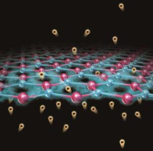
In the latest study, researchers in the NanoPhoton Center at the Technical University of Denmark (DTU) fabricated their nanoscale optical cavity from silicon, the dielectric material workhouse material of modern information technology. Like other such cavities, the new nanostructure is designed to retain light by reflecting it back and forth between two mirrors so that it does not propagate as it usually would.
To design the cavity, the researchers used a technique called topology optimization that was pioneered by team member Ole Sigmund, who initially used it to design bridges and aircraft wings. “Rather than starting with a design concept and then perhaps adding some elements of numerical optimization around this starting point, we let a computer find the optimum design – that is, the one that compresses light most intensely in the optical cavity,” explains team leader Søren Stobbe.
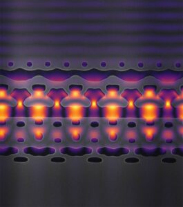
The resulting computer-generated cavity design features a bowtie-like structure at its centre that spatially confines the light. A ring-like structure surrounding the bowtie helps boost the cavity’s quality factor – an intrinsic property of resonators that relates to the strength of loss mechanisms.
Nanofabrication challenges
Fabricating this design was difficult, Stobbe says. To construct it, they had to build an 8 nm silicon bridge in the centre of the bowtie structure, which in turn had to be fully etched into the 220 nm silicon device layer with near-vertical sidewalls. This would be a demanding nanofabrication task on its own, but the researchers also had to address an even more important challenge: contrary to conventional nanocavities based on, for example, photonic crystals or micropillars, the critical dimension plays a key role for bowtie cavities.
“Indeed, the mode volume of the cavity depends on how small the features a given fabrication process enables,” Stobbe tells Physics World, “but changing the process also changes the optimum design. We solved this by measuring the fabrication constraints and including these in the topology optimization. This approach, which is a first in any field of research or engineering, ensures that we get the smallest possible mode volume given by our fabrication process.”
Atom cavity sees the same photon twice
The work could make it possible to develop energy-saving optical chip architectures for components in data centres, computers and telephones, the researchers say. They are now exploring several new directions, including implanting light emitters inside the silicon. “This would allow [us] to directly measure the enhancement of light–matter interactions over the large bandwidths enabled by our cavities,” Stobbe explains.
Another aspect under investigation will be to push the critical dimension of the cavities, which are already close to the size limit possible. This will require entirely new methods for silicon nanofabrication using self-assembly, which appear to be extremely promising, Stobbe reveals.
The present work is detailed in Nature Communications.
- SEO Powered Content & PR Distribution. Get Amplified Today.
- Platoblockchain. Web3 Metaverse Intelligence. Knowledge Amplified. Access Here.
- Source: https://physicsworld.com/a/worlds-smallest-photon-confined-in-dielectric-nanocavity/
- a
- address
- aircraft
- already
- and
- appear
- approach
- around
- aspect
- back
- based
- Better
- between
- boost
- Bowtie
- BRIDGE
- bridges
- build
- called
- cannot
- Center
- centre
- challenge
- Changes
- changing
- chip
- Close
- Columbia
- components
- computer
- computer-generated
- computers
- concept
- constraints
- construct
- consume
- contrary
- conventional
- could
- critical
- data
- data centres
- Date
- demanding
- Denmark
- depends
- Design
- designed
- detailed
- develop
- Development
- device
- difficult
- Dimension
- dimensions
- directly
- elements
- enables
- energy
- Engineering
- ensures
- entirely
- Even
- example
- Explains
- Exploring
- extremely
- Features
- field
- Find
- First
- first time
- Focus
- focused
- from
- fully
- get
- given
- Half
- helps
- How
- However
- HTTPS
- image
- important
- in
- Including
- information
- information technology
- initially
- interactions
- interacts
- intrinsic
- investigation
- issue
- IT
- Key
- large
- latest
- layer
- leader
- leading
- Led
- light
- LIMIT
- loss
- losses
- made
- make
- material
- materials
- Matter
- max-width
- measure
- measuring
- member
- metal
- methods
- Michael
- Middle
- Mode
- Modern
- more
- most
- Nature
- New
- ONE
- optics
- optimization
- optimum
- Other
- own
- perhaps
- picture
- plato
- Plato Data Intelligence
- PlatoData
- Point
- possible
- prediction
- present
- Problem
- process
- promising
- promote
- property
- Push
- quality
- recent
- require
- research
- researchers
- Resolution
- result
- resulting
- Reveals
- Role
- same
- Scale
- sees
- several
- should
- Silicon
- since
- Size
- small
- smaller
- So
- some
- Starting
- States
- store
- strength
- strongly
- structure
- Study
- such
- Surrounding
- Task
- team
- Technical
- Technology
- tells
- The
- their
- theoretical
- thumbnail
- time
- to
- true
- TURN
- under
- university
- us
- usually
- Vacuum
- View
- volume
- which
- WHO
- will
- Work
- would
- years
- zephyrnet