A new technical paper titled “Vertical GeSn nanowire MOSFETs for CMOS beyond silicon” was published by researchers at Peter Grünberg Institute 9, JARA, RWTH Aachen University, CEA, LETI, University of Grenoble Alpes, University of Leeds, and IHP.
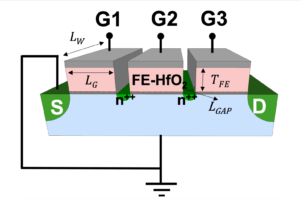
“Here, we present high performance, vertical nanowire gate-all-around FETs based on the GeSn-material system grown on Si. While the p-FET transconductance is increased to 850 µS/µm by exploiting the small band gap of GeSn as source yielding high injection velocities, the mobility in n-FETs is increased 2.5-fold compared to a Ge reference device, by using GeSn as channel material. The potential of the material system for a future beyond Si CMOS logic and quantum computing applications is demonstrated via a GeSn inverter and steep switching at cryogenic temperatures, respectively,” states the paper.
Find the technical paper here. Published February 2023.
Liu, M., Junk, Y., Han, Y. et al. Vertical GeSn nanowire MOSFETs for CMOS beyond silicon. Commun Eng 2, 7 (2023). https://doi.org/10.1038/s44172-023-00059-2.
- SEO Powered Content & PR Distribution. Get Amplified Today.
- Platoblockchain. Web3 Metaverse Intelligence. Knowledge Amplified. Access Here.
- Source: https://semiengineering.com/vertical-nanowire-gate-all-around-fets-based-on-the-gesn-material-system-grown-on-si/
- :is
- 2023
- 7
- 9
- a
- AL
- and
- applications
- AS
- At
- BAND
- based
- Beyond
- by
- Channel
- compared
- computing
- cryogenic
- demonstrated
- device
- February
- For
- future
- gap
- ge
- grown
- High
- HTTPS
- in
- increased
- Institute
- material
- mobility
- Nature
- New
- of
- on
- Paper
- performance
- Peter
- plato
- Plato Data Intelligence
- PlatoData
- potential
- present
- published
- Quantum
- quantum computing
- quantum computing applications
- researchers
- respectively
- Silicon
- small
- Source
- States
- system
- Technical
- The
- titled
- to
- university
- via
- while
- yielding
- zephyrnet