Spintronics at BESSY II: Domain walls in magnetic nanowires
by Sergio Valencia
Berlin, Germany (SPX) Jun 02, 2023
In a breakthrough that could revolutionize spintronic devices, an international team of scientists from Spain, France, and Germany have demonstrated a significant increase in electrical resistance linked to magnetic domain walls in a specific class of materials known as half metals. Among these, a compound named La2/3Sr1/3MnO3 (LSMO) is of particular interest due to its unique properties.
Electrical resistance can vary in spintronic devices based on the presence or absence of magnetic domain walls. This binary effect, referred to as domain wall magnetoresistance, presents an attractive opportunity for encoding information in spintronic memory devices. However, the typical changes in resistance observed for normal ferromagnets such as cobalt have been too small to make practical use of this phenomenon.
LSMO is different. These half metals are part of the manganite perovskite family of compounds and are characterized by full spin polarization, meaning they present only one type of spin. It’s this unique characteristic that has led researchers to believe LSMO could amplify the domain wall magnetoresistance effect significantly, paving the way for a new generation of spintronic sensors and injectors.
The international team successfully created a single domain wall on an LSMO nanowire and recorded changes in resistance that were 20 times larger than those observed for a standard ferromagnet such as cobalt. When a domain wall was present, the electrical resistance increased by up to 12%. This finding resolves some of the previous discrepancies reported in the values of the domain wall magnetoresistance for LSMO.
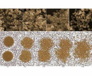
The project was a culmination of a longstanding collaborative effort involving a wide range of techniques including film growth and nanofabrication, transport measurements, contact microscopy (MFM) imaging, theoretical simulations, and advanced characterization techniques such as X-ray photoemission electron microscopy. This multi-pronged approach provided a comprehensive insight into the complex issue and offered new understandings of a hotly debated topic in the field of spintronics.
Related Links
Helmholtz-Zentrum Berlin
Computer Chip Architecture, Technology and Manufacture
Nano Technology News From SpaceMart.com
- SEO Powered Content & PR Distribution. Get Amplified Today.
- PlatoAiStream. Web3 Data Intelligence. Knowledge Amplified. Access Here.
- Minting the Future w Adryenn Ashley. Access Here.
- Buy and Sell Shares in PRE-IPO Companies with PREIPO®. Access Here.
- Source: https://www.spacedaily.com/reports/Spintronics_at_BESSY_II_Domain_walls_in_magnetic_nanowires_999.html
- :has
- :is
- $UP
- 1
- 180
- 20
- 2023
- a
- advanced
- among
- an
- and
- approach
- architecture
- ARE
- AS
- At
- attractive
- based
- been
- believe
- breakthrough
- by
- CAN
- Changes
- characteristic
- characterized
- chip
- class
- collaborative
- COM
- commercial
- complex
- Compound
- comprehensive
- contact
- could
- created
- demonstrated
- Devices
- different
- domain
- due
- effect
- effort
- Expo
- family
- field
- Film
- finding
- For
- France
- from
- full
- generation
- Germany
- Growth
- Half
- Have
- Highlight
- However
- HTML
- http
- HTTPS
- ii
- Imaging
- in
- Including
- Increase
- increased
- information
- insight
- interest
- International
- into
- involving
- issue
- IT
- ITS
- jpg
- known
- larger
- LAS
- Las Vegas
- Led
- linked
- make
- materials
- meaning
- measurements
- Memory
- Metals
- Microscopy
- Named
- New
- news
- normal
- of
- offered
- on
- ONE
- only
- Opportunity
- or
- part
- particular
- Paving
- phenomenon
- plato
- Plato Data Intelligence
- PlatoData
- Practical
- presence
- present
- presents
- previous
- project
- properties
- provided
- range
- recorded
- referred
- Reported
- researchers
- Resistance
- revolutionize
- s
- scientists
- sensors
- significant
- significantly
- single
- small
- some
- Spain
- specific
- Spin
- spx
- standard
- Successfully
- such
- team
- techniques
- Technology
- technology news
- than
- that
- The
- theoretical
- These
- they
- this
- those
- times
- to
- too
- topic
- transport
- type
- typical
- UAV
- unique
- use
- Values
- VEGAS
- Wall
- was
- Way..
- were
- when
- wide
- Wide range
- x-ray
- zephyrnet


