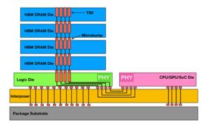
3D stacking of 2D materials
Researchers from Penn State University demonstrated monolithic 3D integration with 2D transistors made from 2D semiconductors called transition metal dichalcogenides. The 2D materials have unique electronic and optical properties, including sensitivity to light, making them ideal for use as sensors.
“One challenge is the process temperature ceiling of 450 degrees Celsius (C) for back-end integration for silicon-based chips — our monolithic 3D integration approach drops that temperate significantly to less than 200 C,” said Darsith Jayachandran, graduate research assistant in engineering science and mechanics at Penn State, in a release. “Incompatible process temperature budgets make monolithic 3D integration challenging with silicon chips, but 2D materials can withstand temperatures needed for the process.”
The 2D materials also showed high carrier mobility and their thinness enabled the researchers to put 30,000 transistors in each tier. [1]
Physical reservoir computing
Researchers at the Tokyo University of Science developed an optical device with features that support physical reservoir computing and allow real-time signal processing across a broad range of timescales within a single device.
The device uses Sn-doped In2O3 and Nb-doped SrTiO3 (ITO/Nb:STO), which responds to both electrical and optical signals. They tested the electrical features of the device to confirm that it functions as a memristor. By varying the voltage and observing changes in the current, the team also explored the influence of ultraviolet light on ITO/Nb:STO. The results suggested that the device can modify the relaxation time of the photo-induced current according to the voltage, making it a potential candidate for a physical reservoir.
When tested on classifying handwritten digit images, the device achieved a classification accuracy of up to 90.2%, compared to an accuracy of 85.1% without the physical reservoir. [2]
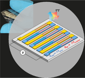
Substrate-integrated TECs
Researchers from University College Cork propose a thermal management approach that combines through glass vias (TGVs) in glass substrates with micro-thermoelectric coolers (micro-TECs) placed underneath a chip.
The substrate integrated micro-thermoelectric coolers (SimTEC) involve TGVs partially filled with copper and thermoelectric materials to provide thermal stabilization of photonic and electronic chips in the package. The method could complement system-level cooling. Simulations indicated a maximum cooling of 9.3 K or a temperature stabilization range of 18.6 K. [3]
References
[1] Jayachandran, D., Pendurthi, R., Sadaf, M.U.K. et al. Three-dimensional integration of two-dimensional field-effect transistors. Nature 625, 276–281 (2024). https://doi.org/10.1038/s41586-023-06860-5
[2] Y. Yamazaki, K. Kinoshita, Photonic Physical Reservoir Computing with Tunable Relaxation Time Constant. Adv. Sci. 2023, 2304804. https://doi.org/10.1002/advs.202304804
[3] Parnika Gupta, Amit Tanwar, Xiuyun He, Kamil Gradkowski, Kafil M. Razeeb, Padraic E. Morrissey, Peter O’Brien, “Substrate integrated micro-thermoelectric coolers in glass substrate for next-generation photonic packages,” J. Optical Microsystems 4(1) 011006 (5 January 2024) https://doi.org/10.1117/1.JOM.4.1.011006

Jesse Allen
Jesse Allen is the Knowledge Center administrator and a senior editor at Semiconductor Engineering.
- SEO Powered Content & PR Distribution. Get Amplified Today.
- PlatoData.Network Vertical Generative Ai. Empower Yourself. Access Here.
- PlatoAiStream. Web3 Intelligence. Knowledge Amplified. Access Here.
- PlatoESG. Carbon, CleanTech, Energy, Environment, Solar, Waste Management. Access Here.
- PlatoHealth. Biotech and Clinical Trials Intelligence. Access Here.
- Source: https://semiengineering.com/research-bits-jan-16/
- :is
- $UP
- 000
- 1
- 16
- 2%
- 200
- 2023
- 2024
- 28
- 2D
- 2D materials
- 30
- 3d
- 80
- 9
- 90
- a
- AC
- According
- accuracy
- achieved
- across
- AL
- All
- All Posts
- allen
- allow
- also
- alternative
- an
- and
- approach
- AS
- Assistant
- At
- Back-end
- both
- broad
- Budgets
- but
- by
- called
- CAN
- candidate
- ceiling
- Celsius
- Center
- challenge
- challenging
- Changes
- chip
- Chips
- classification
- College
- combines
- compared
- Complement
- computing
- Confirm
- constant
- Copper
- could
- Current
- demonstrated
- developed
- device
- Digit
- Drops
- e
- E&T
- each
- editor
- Electronic
- enabled
- Engineering
- Explored
- Features
- filled
- For
- from
- functions
- glass
- graduate
- Gupta
- Have
- he
- High
- HTML
- HTTPS
- ideal
- images
- in
- Including
- indicated
- influence
- integrated
- integration
- involve
- IT
- Jan
- January
- jpg
- knowledge
- less
- light
- made
- make
- Making
- materials
- maximum
- mechanics
- metal
- method
- mobility
- modify
- Monolithic
- Nature
- needed
- next-generation
- of
- on
- or
- our
- package
- packages
- Penn
- Peter
- physical
- placed
- plato
- Plato Data Intelligence
- PlatoData
- Posts
- potential
- process
- processing
- properties
- propose
- provide
- put
- R
- range
- real-time
- relaxation
- release
- research
- researchers
- Results
- Said
- SCI
- Science
- semiconductor
- Semiconductors
- senior
- Sensitivity
- sensors
- showed
- Signal
- signals
- significantly
- Silicon
- single
- stacking
- State
- STO
- support
- team
- tested
- text
- than
- that
- The
- their
- Them
- thermal
- they
- three-dimensional
- Through
- thumbnail
- tier
- time
- to
- tokyo
- transition
- U.K.
- underneath
- unique
- university
- use
- uses
- varying
- Voltage
- which
- with
- within
- without
- zephyrnet