Home > Press > Ribbons of graphene push the material’s potential: A new technique developed at Columbia offers a systematic evaluation of twist angle and strain in layered 2D materials
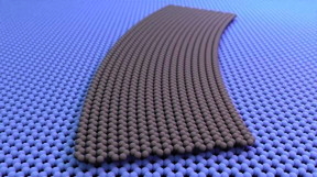 |
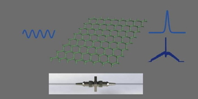
| A curved graphene ribbon, illustrated in grey, shown laid flat against another graphene sheet. There is a continuous change in the twist angle between the ribbon above and the sheet below. In some places the atomic lattices of the two sheets line up at a 0° angle to each other, while in others, they are twisted relative to each other by as much as 5°. CREDIT Cory Dean, Columbia University |
Abstract:
Think you know everything about a material? Try giving it a twist—literally. That’s the main idea of an emerging field in condensed matter physics called “twistronics,” which has researchers drastically changing the properties of 2D materials, like graphene, with subtle changes—as small as going from a 1.1° to 1.2°—in the angle between stacked layers. Twisted layers of graphene, for example, have been shown to behave in ways that single sheets have not, including acting like magnets, like electrical superconductors, or like a superconductor’s opposite, insulators, all due to small changes in the twist angle between sheets.
Ribbons of graphene push the material’s potential: A new technique developed at Columbia offers a systematic evaluation of twist angle and strain in layered 2D materials
New York, NY | Posted on August 11th, 2023
In theory, you could dial in any property by turning a knob that changes the twist angle. The reality, however, isn’t so straightforward, says Columbia physicist Cory Dean. Two twisted layers of graphene can become like a new material, but exactly why these different properties manifest is not well understood, let alone something that can be fully controlled yet.
Dean and his lab have come up with a simple new fabrication technique that may help physicists probe the fundamental properties of twisted layers of graphene and other 2D materials in a more systematic and reproducible way. Writing in Science, they use long “ribbons” of graphene, rather than square flakes, to create devices that offer a new level of predictability and control over both twist angle and strain.
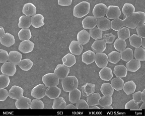
Graphene devices have typically been assembled from atom-thin flakes of graphene that are just a few square micrometers. The resulting twist angle between the sheets is fixed in place, and the flakes can be tricky to layer together smoothly. “Imagine graphene as pieces of saran wrap—when you put two pieces together you get random little wrinkles and bubbles,” says postdoc Bjarke Jessen, a co-author on the paper. Those bubbles and wrinkles are akin to changes in the twist angle between the sheets and the physical strain that develops in between and can cause the material to buckle, bend, and pinch randomly. All these variations can yield new behaviors, but they have been difficult to control within and between devices.
Ribbons can help smooth things out. The lab’s new research shows that, with just a little push from the tip of an atomic force microscope, they can bend a graphene ribbon into a stable arc that can then be placed flat on top of a second, uncurved, graphene layer. The result is a continuous variation in the twist angle between the two sheets that spans from 0° to 5° across the length of the device, with evenly distributed strain throughout—no more random bubbles or wrinkles to contend with. “We no longer have to make 10 separate devices with 10 different angles to see what happens,” said postdoc and co-author Maëlle Kapfer. “And, we can now control for strain, which was completely lacking in prior twisted devices.”
The team used special high-resolution microscopes to confirm how uniform their devices were. With that spatial information, they developed a mechanical model that predicts twist angles and strain values simply based on the shape of the curved ribbon.
This first paper was focused on characterizing the behavior and properties of ribbons of graphene as well as other materials that can be thinned to single layers and stacked on top of each other. “It’s worked with every 2D material that we’ve tried so far,” noted Dean. From here, the lab plans to use their new technique to explore how the fundamental properties of quantum materials change as a function of twist angle and strain. For example, prior research has shown that two twisted layers of graphene act like a superconductor when the twist angle is 1.1. However, there are competing models to explain the origins of superconductivity at this so-called “magic angle,” as well as predictions of additional magic angles that have thus far been too difficult to stabilize, Dean said. With devices made with ribbons, which contain all angles between 0° and 5°, the team can more precisely explore the origins of this phenomenon, and others.
“What we are doing is like quantum alchemy: taking a material and turning it into something else. We now have a platform to systematically explore how that happens,” said Jessen.
####
For more information, please click here
Contacts:
Ellen Neff
Columbia University
Office: 212-853-8048
Copyright © Columbia University
If you have a comment, please Contact us.
Issuers of news releases, not 7th Wave, Inc. or Nanotechnology Now, are solely responsible for the accuracy of the content.
Bookmark:


| Related Links |
| Related News Press |
2 Dimensional Materials
![]() University of Chicago scientists invent smallest known way to guide light: 2D optical waveguides could point way to new technology August 11th, 2023
University of Chicago scientists invent smallest known way to guide light: 2D optical waveguides could point way to new technology August 11th, 2023
![]() Two types of ultrafast mode-locking operations generation from an Er-doped fiber laser based on germanene nanosheets July 21st, 2023
Two types of ultrafast mode-locking operations generation from an Er-doped fiber laser based on germanene nanosheets July 21st, 2023
![]() Understanding the diverse industrial applications of materials science: Materials Science A Field of Diverse Industrial Applications July 21st, 2023
Understanding the diverse industrial applications of materials science: Materials Science A Field of Diverse Industrial Applications July 21st, 2023
News and information
![]() Femtosecond laser technique births “dancing microrobots”: USTC’s breakthrough in multi-material microfabrication August 11th, 2023
Femtosecond laser technique births “dancing microrobots”: USTC’s breakthrough in multi-material microfabrication August 11th, 2023
![]() USTC achieved dynamic imaging of interfacial electrochemistry August 11th, 2023
USTC achieved dynamic imaging of interfacial electrochemistry August 11th, 2023
![]() Simple ballpoint pen can write custom LEDs August 11th, 2023
Simple ballpoint pen can write custom LEDs August 11th, 2023
![]() Chloride ions from seawater eyed as possible lithium replacement in batteries of the future August 11th, 2023
Chloride ions from seawater eyed as possible lithium replacement in batteries of the future August 11th, 2023
Graphene/ Graphite
![]() Two types of ultrafast mode-locking operations generation from an Er-doped fiber laser based on germanene nanosheets July 21st, 2023
Two types of ultrafast mode-locking operations generation from an Er-doped fiber laser based on germanene nanosheets July 21st, 2023
![]() Researchers put a new twist on graphite July 21st, 2023
Researchers put a new twist on graphite July 21st, 2023
Possible Futures
![]() USTC achieved dynamic imaging of interfacial electrochemistry August 11th, 2023
USTC achieved dynamic imaging of interfacial electrochemistry August 11th, 2023
![]() Simple ballpoint pen can write custom LEDs August 11th, 2023
Simple ballpoint pen can write custom LEDs August 11th, 2023
![]() Chloride ions from seawater eyed as possible lithium replacement in batteries of the future August 11th, 2023
Chloride ions from seawater eyed as possible lithium replacement in batteries of the future August 11th, 2023
![]() Tattoo technique transfers gold nanopatterns onto live cells August 11th, 2023
Tattoo technique transfers gold nanopatterns onto live cells August 11th, 2023
Discoveries
![]() Simple ballpoint pen can write custom LEDs August 11th, 2023
Simple ballpoint pen can write custom LEDs August 11th, 2023
![]() Chloride ions from seawater eyed as possible lithium replacement in batteries of the future August 11th, 2023
Chloride ions from seawater eyed as possible lithium replacement in batteries of the future August 11th, 2023
![]() Tattoo technique transfers gold nanopatterns onto live cells August 11th, 2023
Tattoo technique transfers gold nanopatterns onto live cells August 11th, 2023
Materials/Metamaterials/Magnetoresistance
![]() Ultrafast lasers for materials processing August 11th, 2023
Ultrafast lasers for materials processing August 11th, 2023
![]() Understanding the diverse industrial applications of materials science: Materials Science A Field of Diverse Industrial Applications July 21st, 2023
Understanding the diverse industrial applications of materials science: Materials Science A Field of Diverse Industrial Applications July 21st, 2023
![]() A non-covalent bonding experience: Scientists discover new structures for unique hybrid materials by altering their chemical bonds July 21st, 2023
A non-covalent bonding experience: Scientists discover new structures for unique hybrid materials by altering their chemical bonds July 21st, 2023
![]() Researchers put a new twist on graphite July 21st, 2023
Researchers put a new twist on graphite July 21st, 2023
Announcements
![]() Simple ballpoint pen can write custom LEDs August 11th, 2023
Simple ballpoint pen can write custom LEDs August 11th, 2023
![]() Chloride ions from seawater eyed as possible lithium replacement in batteries of the future August 11th, 2023
Chloride ions from seawater eyed as possible lithium replacement in batteries of the future August 11th, 2023
![]() Tattoo technique transfers gold nanopatterns onto live cells August 11th, 2023
Tattoo technique transfers gold nanopatterns onto live cells August 11th, 2023
Interviews/Book Reviews/Essays/Reports/Podcasts/Journals/White papers/Posters
![]() Simple ballpoint pen can write custom LEDs August 11th, 2023
Simple ballpoint pen can write custom LEDs August 11th, 2023
![]() Chloride ions from seawater eyed as possible lithium replacement in batteries of the future August 11th, 2023
Chloride ions from seawater eyed as possible lithium replacement in batteries of the future August 11th, 2023
![]() Tattoo technique transfers gold nanopatterns onto live cells August 11th, 2023
Tattoo technique transfers gold nanopatterns onto live cells August 11th, 2023
- SEO Powered Content & PR Distribution. Get Amplified Today.
- PlatoData.Network Vertical Generative Ai. Empower Yourself. Access Here.
- PlatoAiStream. Web3 Intelligence. Knowledge Amplified. Access Here.
- PlatoESG. Automotive / EVs, Carbon, CleanTech, Energy, Environment, Solar, Waste Management. Access Here.
- PlatoHealth. Biotech and Clinical Trials Intelligence. Access Here.
- ChartPrime. Elevate your Trading Game with ChartPrime. Access Here.
- BlockOffsets. Modernizing Environmental Offset Ownership. Access Here.
- Source: http://www.nanotech-now.com/news.cgi?story_id=57380
- :has
- :is
- :not
- $UP
- 1
- 10
- 21st
- 2D
- 2D materials
- 30
- 7th
- a
- About
- above
- accuracy
- achieved
- across
- Act
- acting
- Additional
- against
- Alchemy
- All
- alone
- an
- and
- Another
- any
- Application
- applications
- Arc
- ARE
- AS
- assembled
- At
- AUGUST
- based
- batteries
- BE
- become
- been
- below
- between
- both
- breakthrough
- but
- by
- called
- CAN
- Cause
- Center
- CGI
- change
- Changes
- changing
- chemical
- chicago
- click
- Co-Author
- Columbia
- COM
- come
- comment
- competing
- completely
- Condensed matter
- Confirm
- content
- continuous
- control
- controlled
- could
- create
- credit
- custom
- Dancing
- developed
- develops
- device
- Devices
- different
- difficult
- discover
- distributed
- diverse
- doing
- drastically
- due
- dynamic
- each
- Electronic
- else
- emerging
- end
- Ether (ETH)
- evaluation
- evenly
- Every
- everything
- exactly
- example
- experience
- Explain
- explore
- far
- few
- field
- First
- fixed
- flat
- focused
- For
- Force
- from
- fully
- function
- fundamental
- generation
- get
- gif
- Giving
- going
- Gold
- Graphene
- guide
- happens
- Have
- help
- here
- high-resolution
- his
- How
- However
- http
- HTTPS
- Hybrid
- idea
- if
- Imaging
- in
- Inc.
- Including
- industrial
- information
- into
- IT
- jpg
- July
- just
- Know
- known
- lab
- lacking
- laser
- lasers
- layer
- layered
- layers
- Length
- Level
- light
- like
- Line
- links
- lithium
- little
- live
- Long
- longer
- made
- magic
- Magnets
- Main
- make
- material
- materials
- Matter
- May..
- mechanical
- Microscope
- model
- models
- more
- much
- nanotechnology
- net
- New
- New York
- news
- no
- Noise
- noted
- now
- NY
- of
- offer
- Offers
- on
- Operations
- opposite
- or
- origins
- Other
- Others
- out
- over
- Paper
- phenomenon
- PHP
- physical
- Physics
- pieces
- Place
- Places
- plans
- platform
- plato
- Plato Data Intelligence
- PlatoData
- please
- Point
- possible
- Post
- posted
- potential
- precisely
- Predictions
- Predicts
- press
- Press Release
- Prior
- probe
- properties
- property
- Push
- put
- Quantum
- quantum materials
- random
- rather
- Reality
- relative
- release
- Releases
- replacement
- research
- researchers
- responsible
- result
- resulting
- return
- Ribbon
- s
- Said
- Save
- says
- Science
- scientists
- Search
- Second
- see
- Semiconductors
- separate
- Shape
- Share
- sheet
- shown
- Shows
- Simple
- simply
- single
- small
- smooth
- smoothly
- So
- so Far
- solely
- some
- something
- spans
- Spatial
- special
- square
- stabilize
- stable
- stacked
- start
- straightforward
- submit
- Superconductivity
- taking
- team
- than
- that
- The
- their
- then
- theory
- There.
- These
- they
- things
- this
- those
- Thus
- tip
- to
- together
- too
- top
- transfers
- tried
- try
- Turning
- twist
- two
- types
- typically
- understood
- unique
- university
- unwanted
- us
- use
- used
- USTC
- Values
- Voltage
- was
- Wave
- Way..
- ways
- we
- WELL
- were
- What
- when
- which
- while
- why
- with
- within
- worked
- write
- writing
- Yahoo
- yet
- Yield
- york
- you
- zephyrnet