News: Suppliers
8 September 2023
Korea Electrotechnology Research Institute (KERI) — which is funded under the National Research Council of Science & Technology (NST) of South Korea’s Ministry of Science and ICT — has transferred ion implantation and evaluation technology for silicon carbide (SiC) power semiconductors to metrology equipment firm SEMILAB ZRT of Budapest, Hungary.
While SiC power semiconductors have many advantages, the manufacturing process is very challenging. Previously, the method was to create a device by forming an epitaxial layer on a highly conductive wafer and flowing current through that area. However, during this process, the surface of the epilayer becomes rough and the speed of electron transfer decreases. The price of the epiwafer itself is also high, which is a major obstacle to mass production.
To solve this problem, KERI used a method of implanting ions into a semi-insulating SiC wafer without an epilayer in order to make the wafer conductive.
Since SiC materials are hard, they require very high-energy ion implantation followed by high-temperature heat treatment to activate the ions, making it a difficult technology to implement. However, KERI says that, based on its 10 years of experience in operating ion implantation equipment dedicated to SiC, it has succeeded in establishing the relevant technologies.

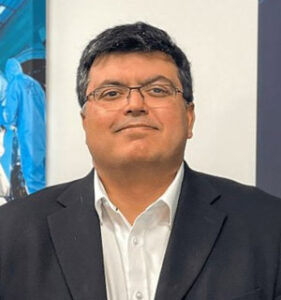
Picture: Second from left, Dr Bahng Wook, executive director of KERI’s Power Semiconductor Research Division; third from the left, Park Su-yong, CEO of Semilab Korea Co Ltd.
“Ion implantation technology can significantly reduce process costs by increasing current flow in semiconductor devices and replacing expensive epiwafers,” says Dr Kim Hyoung Woo, director, Advanced Semiconductor Research Center, KERI. “This is a technology that increases the price competitiveness of high-performance SiC power semiconductors and contributes greatly to mass production.”
The technology was recently transferred to SEMILAB, which has manufacturing plants in Hungary and the USA. With a 30-year history, SEMILAB owns patents for medium-sized precision measurement equipment and material characterization equipment, and possesses technology for semiconductor electrical parameter evaluation systems.

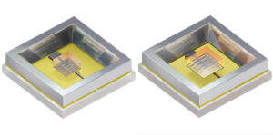
Picture: Semi-insulating SiC wafer.
The firms expect that, through the technology transfer, they will be able to standardize high-quality SiC. SEMILAB plans to use KERI’s technology to develop specialized equipment to evaluate the ion implantation process for SiC power semiconductors. “Through the development of specialized equipment, we will be able to progress in-line monitoring of implant processes on SiC wafers for immediate, accurate and low-cost production control of implant systems and in-line monitoring for pre-anneal implant,” says Park Su-yong, president of SEMILAB Korea. “This will be a great foundation for stably securing a high-quality ion implantation mass-production process with excellent uniformity and reproducibility.”
SiC devices Power electronics ion implanters
- SEO Powered Content & PR Distribution. Get Amplified Today.
- PlatoData.Network Vertical Generative Ai. Empower Yourself. Access Here.
- PlatoAiStream. Web3 Intelligence. Knowledge Amplified. Access Here.
- PlatoESG. Automotive / EVs, Carbon, CleanTech, Energy, Environment, Solar, Waste Management. Access Here.
- PlatoHealth. Biotech and Clinical Trials Intelligence. Access Here.
- ChartPrime. Elevate your Trading Game with ChartPrime. Access Here.
- BlockOffsets. Modernizing Environmental Offset Ownership. Access Here.
- Source: https://www.semiconductor-today.com/news_items/2023/sep/keri-semilabzrt-080923.shtml
- :has
- :is
- 10
- a
- Able
- accurate
- advanced
- advantages
- also
- an
- and
- ARE
- AREA
- based
- BE
- becomes
- Budapest
- by
- CAN
- Center
- ceo
- challenging
- CO
- COM
- competitiveness
- contributes
- control
- Costs
- Council
- create
- Current
- decreases
- dedicated
- develop
- Development
- device
- Devices
- difficult
- Director
- Division
- dr
- during
- equipment
- establishing
- Ether (ETH)
- evaluate
- evaluation
- excellent
- executive
- Executive Director
- expect
- expensive
- experience
- Firm
- firms
- flow
- Flowing
- followed
- For
- Foundation
- from
- funded
- great
- greatly
- Hard
- Have
- High
- high-performance
- high-quality
- highly
- history
- However
- http
- HTTPS
- Hungary
- ICT
- immediate
- implement
- in
- Increases
- increasing
- Institute
- into
- IT
- ITS
- itself
- jpg
- Kim
- korea
- Korea’s
- layer
- left
- low-cost
- Ltd
- major
- make
- Making
- manufacturing
- many
- Mass
- material
- materials
- measurement
- method
- Metrology
- ministry
- monitoring
- National
- obstacle
- of
- on
- operating
- order
- owns
- parameter
- Park
- Patents
- plans
- plants
- plato
- Plato Data Intelligence
- PlatoData
- power
- Precision
- president
- previously
- price
- Problem
- process
- processes
- Production
- Progress
- RE
- recently
- reduce
- relevant
- require
- research
- says
- Science
- Second
- securing
- semiconductor
- Semiconductors
- September
- significantly
- Silicon
- silicon carbide
- SOLVE
- South
- specialized
- speed
- Surface
- Systems
- Technologies
- Technology
- that
- The
- they
- Third
- this
- Through
- to
- transfer
- transferred
- transfers
- treatment
- under
- USA
- use
- used
- very
- was
- we
- which
- will
- with
- without
- Woo
- years
- zephyrnet