Quest for an ideal switching device for ultra-low power applications leads to an exploration of novel micro/nanoelectromechanical systems (M/NEMS) switches. This research has been driven by the superior performance of M/NEMS devices, such as ideally abrupt switching with zero off-state leakage, suitable for harsh and extreme environments, and very small footprints.
The suspended element of the NEMS switch is electro-mechanically moved by the applied electric field to establish physical contact with the counterpart of the switch, and thereby the conducting channel is established.
However, an unacceptably high switching voltage of NEMS switches is the main obstacle to their practical use of it in low-power integrated circuits. In particular, sub-0.5 V switching voltage with a very small switch footprint, which is needed for ultra-low power circuits, has not yet been demonstrated because of irreversible switching failure caused by surface adhesion.
Moreover, once physical contact is created in NEMS switches, the switch contact area is increased, which leads to the domination of the surface attraction force over the mechanical restoring force; and as a result, permanent adhesion occurs.
To succeed in the realizing NEMS switch for ultra-low power applications, the thickness of movable suspended material thickness has to be reduced as well as the switch contact adhesion in the ON state has to be overcome to reach the OFF state.
The research team led by Dr. Manoharan Muruganathan (Former Senior Lecturer), and Professor Hiroshi Mizuta at the Japan Advanced Institute of Science and Technology (JAIST) proposed graphene-based NEMS switch research for this purpose.
In the NEMS switch, the switching voltage is directly proportional to the suspended beam thickness, whereas the graphene monolayer is the thinnest material in the world today. Also, the graphene exhibits cubic mechanical restoring force in the ON state, which is crucial to avoid stiction.
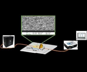
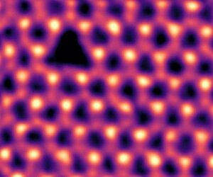
Due to this unique characteristic, this research team pursued the graphene NEMS switch based on the doubly-clamped suspended graphene beam with the hexagonal boron nitride (hBN) contact at the switching terminal.
Graphene-to-hBN binding strength is low due to its van der Waals (vdW) bonding nature, which will overcome the stiction issue of NEMS switches says the researcher Dr. Ngoc Huynh Van of Technical University of Denmark. Based on the unique choice of materials and NEMS switch design, they have demonstrated sub-0.5 V switching characteristics with more than 50,000 hot-switching cycles of operation.
Moreover, these NEMS switches exhibit excellent switching characteristics, such as ~5 mV/dec switching slope, nearly-zero hysteresis, and >105 ON/OFF ratio, which meets the mainstream CMOS technology requirements. These NEMS switches will play a vital role in various NEMS devices, sensors, NEM-CMOS hybrid integrated circuits, and ultralow-power applications.
Research Report:Sub 0.5 Volt Graphene-hBN van der Waals Nanoelectromechanical Switches
Related Links
Japan Advanced Institute of Science and Technology
Computer Chip Architecture, Technology and Manufacture
Nano Technology News From SpaceMart.com
| Thanks for being there; We need your help. The SpaceDaily news network continues to grow but revenues have never been harder to maintain. With the rise of Ad Blockers, and Facebook – our traditional revenue sources via quality network advertising continues to decline. And unlike so many other news sites, we don’t have a paywall – with those annoying usernames and passwords. Our news coverage takes time and effort to publish 365 days a year. If you find our news sites informative and useful then please consider becoming a regular supporter or for now make a one off contribution. |
||
|
SpaceDaily Monthly Supporter $5+ Billed Monthly |
SpaceDaily Contributor $5 Billed Once credit card or paypal |
|

![]()
New quantum computing architecture could be used to connect large-scale devices
Boston MA (SPX) Jan 06, 2023
Quantum computers hold the promise of performing certain tasks that are intractable even on the world’s most powerful supercomputers. In the future, scientists anticipate using quantum computing to emulate materials systems, simulate quantum chemistry, and optimize hard tasks, with impacts potentially spanning finance to pharmaceuticals. However, realizing this promise requires resilient and extensible hardware. One challenge in building a large-scale quantum computer is that researchers must find … read more
- SEO Powered Content & PR Distribution. Get Amplified Today.
- Platoblockchain. Web3 Metaverse Intelligence. Knowledge Amplified. Access Here.
- Source: https://www.spacedaily.com/reports/Graphene_nano_mechanical_switches_could_make_our_electronics_even_smaller_and_ultra_low_power_999.html
- 000
- 1
- 10
- 100
- 11
- 7
- a
- Ad
- advanced
- Advertising
- All
- and
- anticipate
- applications
- applied
- architecture
- AREA
- based
- basket
- Beam
- because
- becoming
- being
- binding
- Building
- card
- caused
- Center
- certain
- challenge
- Channel
- characteristic
- characteristics
- chemistry
- chip
- choice
- computer
- computers
- computing
- conducting
- Connect
- Consider
- contact
- continues
- contribution
- contributor
- could
- coverage
- created
- crucial
- cycles
- Days
- Decline
- demonstrated
- Denmark
- Design
- device
- Devices
- directly
- driven
- effort
- Electric
- Electronics
- environments
- establish
- established
- Even
- excellent
- exhibit
- exhibits
- exploration
- extreme
- Failure
- field
- finance
- Find
- Footprint
- Force
- Former
- from
- future
- Graphene
- Grow
- Hard
- Hardware
- help
- High
- Highlight
- hold
- However
- HTML
- HTTPS
- Hybrid
- ideal
- Impacts
- in
- increased
- informative
- Institute
- integrated
- issue
- IT
- Jan
- Japan
- large-scale
- Leads
- lecturer
- Led
- Low
- Main
- Mainstream
- maintain
- make
- many
- material
- materials
- mechanical
- Meets
- monthly
- more
- most
- Nature
- Need
- needed
- network
- news
- News sites
- novel
- obstacle
- ONE
- operation
- Optimize
- Other
- Overcome
- particular
- Passwords
- performance
- performing
- permanent
- pharmaceuticals
- physical
- plato
- Plato Data Intelligence
- PlatoData
- Play
- please
- potentially
- power
- powerful
- Practical
- Professor
- promise
- proposed
- publish
- purpose
- quality
- Quantum
- Quantum Computer
- quantum computers
- quantum computing
- quest
- ratio
- reach
- realizing
- Reduced
- regular
- report
- Requirements
- requires
- research
- researcher
- researchers
- resilient
- restoring
- result
- revenue
- revenues
- Rise
- Role
- Science
- Science and Technology
- scientists
- senior
- sensors
- Sites
- Slope
- small
- smaller
- So
- Sources
- spx
- State
- strength
- succeed
- such
- suitable
- supercomputers
- superior
- supporter
- Surface
- suspended
- Switch
- Systems
- takes
- tasks
- team
- tech
- Technical
- Technology
- technology news
- Terminal
- The
- The Future
- the world
- their
- thereby
- time
- to
- today
- top
- traditional
- unique
- university
- use
- various
- via
- vital
- Volt
- Voltage
- which
- will
- world
- year
- Your
- zephyrnet
- zero