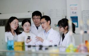
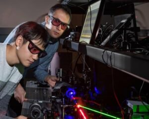
Already this year, Elham Fadaly has completed a PhD and won an award for her work on semiconductor crystal growth mechanisms, which helped to create a silicon-based light emitter. She talks to Tami Freeman about this award-winning research and her plans for the future
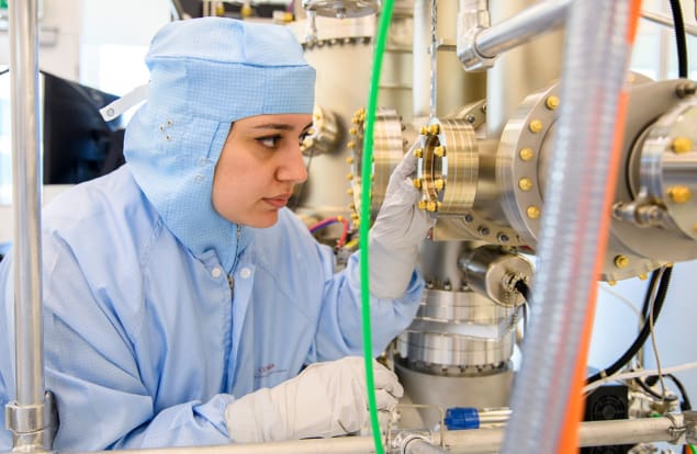
You were runner-up for the Nanotechnology Young Researcher Award, which recognizes early career brilliance. What was the research that led to this award?
I performed this work as part of my PhD at Eindhoven University of Technology. In the field of semiconductor physics, efficient light emission from silicon has been the “Holy Grail” for the past five decades. But despite remarkable efforts in the field, this has not yet been achieved due to silicon’s indirect band gap. Germanium-rich silicon-germanium alloys with a hexagonal crystal structure have been predicted to exhibit a direct band gap and efficient light emission. But the bottleneck here is that silicon and germanium naturally crystallize in a cubic structure and it is challenging to change this into a hexagonal structure.
In our research, we have achieved this by copying the hexagonal crystal structure from a hexagonal template of gallium-arsenide nanowires, which have nearly matching structural properties to our silicon-germanium material. The nanowires act as a unique platform for realizing these new crystal structures, without the material reversing back to its natural cubic structure. And we have created hexagonal silicon-germanium material in large volumes using these gallium-arsenide nanowire templates.
Now that light emission has been achieved, what could be the main applications for this material?
The biggest application, which we are all waiting for, is a silicon-based laser for on-chip and chip-to-chip communications. We have demonstrated efficient band-gap emission from this material; and we have shown the tunability of this emission in the wavelength window 1.8–3.5 μm, close to the optical communications window. These results reveal the strong potential of hexagonal silicon germanium for silicon-based light-emitting devices, hopefully paving the way to uniting electronic and optoelectronic functionalities on a single chip.
We could also use this in lidar systems used, for example, in autonomous driving, biological sensors and solar cells. It is a very promising material that emits and detects in a technologically interesting wavelength range.
While studying this material, you found a new type of crystal defect, what was this?
The hexagonal crystal structure has been synthesized in silicon germanium in the past few years, but only in small volumes. When we fabricated this material with high quality and in very large volumes, we started to see a new type of crystal defect. And when we ran a thorough structural characterization, we identified this as an I3 basal stacking fault.
An I3 basal stacking fault appears like a partial defect – if you look at the crystal under a microscope, you see partial lines running through the material. It is actually a triangular defect, terminated by two partial dislocations. And between those two partial dislocations, separated by 60 ˚, there is a stacking fault where the atoms order in a different manner from the hexagonal ordering.
If you think about it, this hexagonal structure is not the stable, natural form of silicon germanium, so the material tries to minimize its energy by creating these defects. But we have created a deep understanding of the defects, such that we can try to avoid them in the future and fabricate high-quality material by tuning the growth dynamics.
Would such defects cause a problem if they ended up in a device?
We performed optical characterization and saw that the defects do not really deteriorate the optical properties of our material. This is because – as we saw when we theoretically calculated the band structure of these materials – the defect states are created outside the material’s band gap. But of course, if the material is heavily defected by this I3 defect, it may change into the wrong structure. So ultimately, we have to have a very low defect level so that it does not affect the optical properties.
What are you working on now?
The rest of my team is working hard to show lasing from the silicon-germanium material. If we show lasing, this would be another breakthrough. I have just finished my PhD and am embarking upon the next step in my career. I am moving to work as a laser engineer research scientist at Apple in Silicon Valley in California. But hopefully I will stay in the field of optoelectronics and materials; this is really my passion.
Your degree was in electronic engineering – what prompted your move into physics?
As a bachelor student at the American University in Cairo, I was really fond of circuits and electronics. So in the third year of my degree, I travelled to the US as a part of an exchange programme. There I was introduced to the physics of semiconductors and semiconductor devices.
As an engineer, when you’re working with electronic devices, you are almost working with a black box, tuning the input and output and so on. But with physics, you’re really diving deep into the underlying concepts. I felt like I was exploring the hidden world behind electronic devices. And this was a fascinating world for me.
With physics, you’re really diving deep into the underlying concepts. I felt like I was exploring the hidden world behind electronic devices
After coming back to Egypt, I decided to focus more on the physics of semiconductors. And then I started a Master’s degree in nanoscience and nanotechnology. It was still nanoelectronics, but I focused a lot more on physics and nanomaterials courses. My thesis project was on nanomaterials.
You have also been involved with a UN climate change programme. What did that entail?
Since I was young, I have been passionate about community development and engagement activities. When I was still an undergraduate, I was interested in environmental issues and advocating for action on climate change, so I participated in a conference in Indonesia in 2011 as part of the United Nations Environment Programme (UNEP). There, I was nominated and elected as an African youth adviser as part of the UNEP-TUNZA Youth Advisory Council for 2012 and 2013.
I was representing African youth in ministerial meetings, international conferences and international forums concerned with environmental programmes and climate-change issues. It was really a great experience; I learned a lot. I think community development is very complimentary to science, everything goes hand-in-hand.
- SEO Powered Content & PR Distribution. Get Amplified Today.
- EVM Finance. Unified Interface for Decentralized Finance. Access Here.
- Quantum Media Group. IR/PR Amplified. Access Here.
- PlatoAiStream. Web3 Data Intelligence. Knowledge Amplified. Access Here.
- Source: https://physicsworld.com/a/exploring-the-hidden-world-behind-electronic-devices/
- :has
- :is
- :not
- :where
- $UP
- 1
- 2011
- 2012
- 2013
- 60
- a
- About
- about IT
- achieved
- Act
- Action
- activities
- actually
- advisory
- advocating
- affect
- African
- All
- also
- am
- American
- an
- and
- Another
- Apple
- Application
- applications
- ARE
- AS
- At
- autonomous
- avoid
- award
- award-winning
- back
- BAND
- BE
- because
- been
- behind
- between
- Biggest
- Black
- Box
- breakthrough
- but
- by
- calculated
- california
- CAN
- Career
- Cause
- Cells
- challenging
- change
- chip
- Climate
- Climate change
- Close
- coming
- Communications
- community
- Community Development
- Completed
- complimentary
- concepts
- concerned
- Conference
- conferences
- copying
- could
- Council
- course
- courses
- create
- created
- Creating
- Crystal
- decades
- decided
- deep
- Degree
- demonstrated
- Despite
- Development
- device
- Devices
- DID
- different
- direct
- do
- does
- driving
- due
- dynamics
- Early
- efficient
- efforts
- Egypt
- elected
- Electronic
- Electronics
- emission
- energy
- engagement
- engineer
- Engineering
- Environment
- environmental
- everything
- example
- exchange
- exhibit
- experience
- Exploring
- fascinating
- few
- field
- five
- Focus
- focused
- For
- form
- forums
- found
- from
- functionalities
- future
- gap
- Goes
- great
- Growth
- Hard
- Have
- heavily
- helped
- her
- here
- Hidden
- High
- high-quality
- Hopefully
- HTTPS
- i
- identified
- if
- image
- in
- Indonesia
- information
- input
- interested
- interesting
- International
- into
- introduced
- involved
- issue
- issues
- IT
- ITS
- jpg
- lab
- large
- laser
- learned
- Led
- Level
- lidar
- light
- like
- lines
- Look
- Lot
- Low
- Main
- manner
- master’s
- matching
- material
- materials
- max-width
- May..
- mechanisms
- meetings
- Microscope
- more
- move
- moving
- my
- Nanomaterials
- nanotechnology
- Nations
- Natural
- nearly
- New
- next
- now
- of
- on
- only
- order
- our
- output
- outside
- part
- participated
- passion
- passionate
- past
- Paving
- performed
- Physics
- Physics World
- plans
- platform
- plato
- Plato Data Intelligence
- PlatoData
- potential
- predicted
- Problem
- programme
- programmes
- project
- promising
- properties
- quality
- range
- realizing
- really
- recognizes
- remarkable
- representing
- research
- researcher
- REST
- Results
- reveal
- running
- Science
- Scientist
- see
- semiconductor
- Semiconductors
- sensors
- she
- show
- shown
- Silicon
- Silicon Valley
- single
- small
- So
- solar
- Solar cells
- stable
- stacking
- started
- States
- stay
- Step
- Still
- strong
- structural
- structure
- Student
- Studying
- such
- Suit
- surf
- Systems
- Talks
- team
- Technology
- template
- templates
- that
- The
- The Future
- Them
- then
- There.
- These
- thesis
- they
- think
- Third
- this
- this year
- those
- Through
- thumbnail
- to
- true
- try
- two
- type
- Ultimately
- UN
- under
- underlying
- understanding
- unique
- United
- united nations
- university
- upon
- us
- use
- used
- using
- Valley
- very
- volumes
- Waiting
- was
- Way..
- we
- were
- What
- when
- which
- with
- without
- Won
- Work
- working
- world
- would
- Wrong
- year
- years
- yet
- you
- young
- Your
- youth
- zephyrnet

