Device structure and band diagrams of few-layer InSe
To obtain high-quality samples, we encapsulate γ-phase InSe flakes in hBN and use few-layer graphite (FLG) flakes as electrodes. We use a FLG bottom gate to modulate the carrier density in the semiconductor. The complete device schematic is reported in Fig. 1b, representing an optically excited heterostructure based on InSe. In Fig. 1a, an example of a 3L InSe device is shown in false colour to highlight the stacked layers. The band structure for three layers of InSe was obtained by density functional theory (DFT) calculations accounting for the presence of selenium vacancies (VSe), the most common type of defects in few-layer InSe due to their low formation energy19,20 (Supplementary Note 1). These defects produce two peaks in the DOS close to the conduction band and a peak at roughly 150 meV from the valence band, as shown in Fig. 1c,d. In few-layer InSe, a sharp DOS increase characterizes the VBM position (Fig. 1e) due to the appearance of a van Hove singularity.
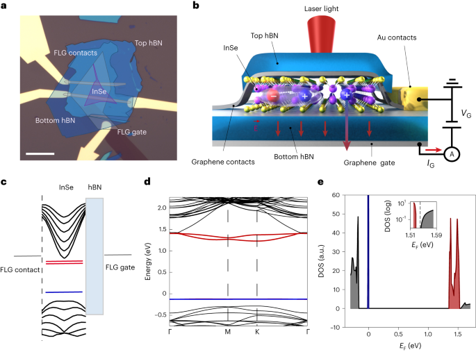
a, Optical microscope picture of the 3L device with layers highlighted in false colour. FLG, InSe and hBN layers are depicted in grey, violet and blue, respectively. Scale bar, 20 μm. b, Three-dimensional schematic representing an hBN-encapsulated InSe layer with graphene contacts and a wide back gate. The sample is optically excited using a red laser and excitonic species are formed within the semiconductor. When a gate voltage is applied, holes in InSe can tunnel through the bottom hBN giving rise to a tunnelling photocurrent. The electrical measurement scheme is shown on the right. c, Band alignment of the materials of interest in the device of Fig. 1b. Two electron donor (red) and one acceptor (blue) states are induced by the presence of selenium vacancies. d, Band structure of the 3L slab of InSe with a selenium vacancy. A van Hove singularity arises due to the band flattening at the Γ point. e, The DOS in a 3L-InSe shows a sharp peak at the VBM, as well as the donor (red) and acceptor (blue) states. The inset shows in logarithmic scale the region between the highest donor state and the beginning of the conduction band, with its minimum located at 1.54 eV with respect to the acceptor state.
By taking defect states into account, we explain the nature of lateral hole transport in InSe devices and the change in tunnelling behaviour at the point corresponding to the flat-band position. Moreover, our calculations reveal valence-band offsets on the order of hundreds of meVs in heterostructures with FLG-contacted few-layer InSe on top of hBN (Fig. 1c and Supplementary Fig. 1), unveiling a notably asymmetrical alignment when compared to the band offsets at the conduction band (roughly 3.8 eV). This asymmetry is crucial for the electrical detection of the DOS at the van Hove singularity at the VBM.
We note that band alignments obtained by DFT calculations are known to be susceptible to variabilities21. Here, we use hybrid and meta-GGA functionals in DFT calculations to gain semiquantitative insights into the highly-asymmetrical band alignment between few-layer InSe and hBN. The calculated values of the band alignment are in the range of hundreds of meV for holes, which further confirms our findings regarding the order of magnitude of the barriers extracted experimentally from tunnelling photocurrent measurements, as presented in the following sections.
Lateral transport and tunnelling photocurrent
On Fig. 2a we present the gate dependence of the lateral current in our 3L and 6L devices. We observe ambipolar transport with dominant n-type transport5,6 while p-type conduction is strongly suppressed due to relatively high hole effective masses compared to the electron ones (Supplementary Table 1). The successful observation of subthreshold p-type lateral currents in our devices is attributed to the combination of using a high-purity InSe crystal source (HQ Graphene) and full hBN-encapsulation with lateral graphene electrodes. This ensures that the InSe flakes are never exposed to air at any point during device handling (Methods). A visible decrease in the p-type subthreshold slope is seen in the 3L with respect to the 6L device, consistent with the reduction of the hole effective mass with an increasing number of InSe layers, as discussed in Supplementary Notes 1 and 2.
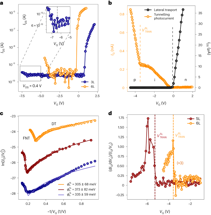
a, Field-effect lateral transport in the 3L (measured at 80 mK) and 6L devices in logarithmic scale. Subthreshold p-type conduction was achieved in both samples. Note a lower subthreshold slope in the 3L with respect to the 6L device (Supplementary Note 2). The inset highlights the onset of p-type conduction in the 3L device (({V}_{mathrm{ON}}^{3{mathrm{L}}}simeq-6.4,{mathrm{V}})). b, The gate-dependent lateral current between the FLG contacts in a 6L device (black) shows predominantly n-type conduction in linear scale. The dashed grey line indicates the onset of n-type conduction. A gate-dependent tunnelling photocurrent is induced when the sample is illuminated using a 633 nm laser at 50 µW of power (yellow). The behaviour of the tunnelling current can be divided into two main regions, which are separated by a yellow dashed line with respect to the gate voltage. c, The gate-dependent tunnelling photocurrent data for 3L, 5L and 6L devices are reported in blue, red and yellow circles, respectively, using the (mathrm{ln}left(|{I}_{mathrm{G}}text{|}/{V}_{mathrm{G}}^{2}right)) scale with respect to −1/VG for VG < −1 V. The tunnelling behaviour is modelled using Simmons’ approximation, with direct tunneling (DT) and FNT regimes separated by a sharp onset. FNT fittings reveal effective barriers for tunnelling holes of 237, 340 and 292 meV for 3L, 5L and 6L samples, respectively. d, Ratio between the differential conductance and the tunnelling conductance at low temperature for 5L and 6L devices. The weaker 3L signal does not allow us to observe changes in the normalized conductance at cryogenic temperature. Further discussion on the temperature dependence of the dIG/dVG signals is provided in Supplementary Note 3.
Illumination of the device with a laser beam (λ = 633 nm) results in the appearance of an out-of-plane tunnelling current between the InSe layers and the FLG gate, shown on Fig. 2b for the 6L device together with the lateral current as a function of gate voltage. The tunnelling current shows a rapid increase at VG = −3.5 V, closely matching the hole conduction onset voltage VON 6L= −3.6 V. Photocurrents for devices with varying thicknesses (3L, five layers (5L) and 6L) are shown in Fig. 2c on a logarithmic scale, revealing two main regions with linear and logarithmic trends, respectively. This behaviour is reminiscent of the separation between direct tunnelling (DT) and Fowler–Nordheim tunnelling (FNT) mechanisms in electronic devices such as metal-insulator-metal diodes22,23 and can be modelled using Simmons’ approximation22,24 (Supplementary Note 3). To perform the fitting under Simmons’ approximation, we have used the measured bottom hBN thicknesses of 20, 25 and 18 nm for the 3L, 5L and 6L devices, respectively (Methods). The FNT part allows us to extract the tunnel barrier heights. We refer to the position of changing trends as the transition voltage VTRAN, which for the 6L device occurs at −3.5 V while for the 3L sample, ({V}_{mathrm{TRAN}}^{3{mathrm{L}}},)= (-5.8,{mathrm{V}}), close to the onset of p-type conductivity ({V}_{mathrm{ON}}^{3{mathrm{L}}}simeq-6.4,{mathrm{V}}).
To rule out the possibility that the drastic change in the tunnelling transition is due to change in the transmission probability, we consider the differential tunnelling conductance dIG/dVG normalized over the total conductance IG/VG (Fig. 2d). As previously reported25, the appearance of a peak in the (dIG/dVG)/(IG/VG) curve indicates that the rise of the tunnelling signal is due to a sudden change in the material DOS (Supplementary Note 3).
Relationship between tunnelling mechanisms and excitons
To understand the sharp transition in the tunnelling photocurrent in the presence of a van Hove singularity at the VBM, we compare tunnelling photocurrent measurements with gate-dependent photoluminescence spectroscopy (Fig. 3a), allowing us to identify different excitonic species and defect-bound states8. We focus our attention on the redshift of the main excitonic species in the p-type region X+, together with its strong suppression of emission for ({V}_{mathrm{G}}^{6{mathrm{L}}} < -3.5,{mathrm{V}}). This corresponds to the Fermi level crossing into the valence band and the accompanying BGR at the flat band. This voltage also coincides with the onset of the tunnelling photocurrent in the 6L device (Fig. 3b) and hole accumulation in the semiconductor. Similar behaviour is shown in Supplementary Note 5 for the 5L device.
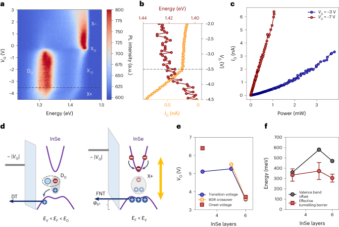
a, Gate-dependent photoluminescence (PL) spectra for the 6L device. The change in the main excitonic peaks with respect to gate voltage is related to different charge configurations (Supplementary Note 4). When the Fermi level in the semiconductor enters the valence band (grey dashed line), the highest energy peak shifts linearly with respect to the gate voltage due to BGR in the presence of a dense hole Fermi sea. b, Peak position of the highest energy excitonic species (red) and tunnelling photocurrent (yellow) in the vicinity of the VBM. The direct tunnelling (DT)-to-FNT transition (({V}_{mathrm{TRAN}}^{5{mathrm{L}}})) and the BGR start (({V}_{mathrm{BGR}}^{5{mathrm{L}}}) are highlighted by dashed yellow and red lines, respectively. c, Power-dependent tunnelling photocurrent for the 5L device (Supplementary Note 5) when the Fermi level lies within the bandgap (blue) or has entered the valence band (red). The superlinear behaviour of the former case indicates that second-order excitonic effects play a role, which is excluded within the valence band. d, Auger and exciton–exciton recombination mechanisms can radiatively transfer their energy to resident carriers and induce hot-hole tunnelling through a thick hBN barrier in the presence of a vertical electric field (EV < EF < ED). When the Fermi level lies within the valence band (EF < EV), excitonic species are subject to interactions with the Fermi sea induced by the high DOS and directly photo-excited holes are responsible for the photocurrent by FNT through the hBN barrier (right). e, Transition voltage (VTRAN), BGR crossover (VBGR) and p-type onset (VON) for the 3L, 5L and 6L devices. The 5L sample was not equipped with two FLG contacts for lateral transport measurements, and the intensity of photoluminescence emission in the 3L sample was too low to be analysed as a function of gate voltage. f, Layer-dependent effective tunnelling barrier extracted from FNT fittings (Fig. 2b) and valence-band offsets obtained from DFT calculations (Supplementary Fig. 1). The effective barrier values are presented as mean values (dots) and corresponding standard deviations (error bars).
In Fig. 3c, we show the excitation power (P) dependence of the tunnelling photocurrent (I) in the p-type region (VG = −7 V) and within the bandgap (VG = −3 V), displaying a linear and a superlinear behaviour, respectively. I ∝ Pα dependence with ɑ ≅ 2 is commonly attributed to second-order mechanisms such as exciton–exciton annihilation26. For 1 < α < 2, first-order recombination pathways also play a role, mainly represented by Auger processes27. Here, non-radiative exciton recombination results in energy transfer to charge carriers, which become sufficiently excited to tunnel through the hBN barrier in the presence of a vertical electric field. The effective tunnelling barrier extracted for the Fowler–Nordheim region lies in the range of several hundred meV for 3L, 5L and 6L devices, with values that are comparable with the calculated valence-band offsets for the respective structures (Supplementary Fig. 1).
Previous reports have shown the excitation of charge carriers through Auger recombination and vertical photocurrent due to hot-carrier tunnelling for other 2D materials24,27,28. However, no DOS-dependent sharp transition between direct tunnelling and FNT regions can be identified in either our TMDC-based samples (Supplementary Note 6) or in the literature, where the increase in photocurrent is attributed to the bending of the hBN bands by an increasing electric field. A different mechanism is therefore needed to explain the sharp transition between direct tunnelling and FNT regions in InSe. In our case, the aforementioned suppression of photoluminescence from X+, together with the reduction of the power coefficient α with the onset of hole conduction, both indicate that exciton densities are reduced when the Fermi level enters the valence band. Since the generation factor is fixed only by the input optical power (Supplementary Note 4), we infer that, in the p-type region, Auger recombination plays a minor role in the tunnelling pathways from InSe through the hBN barrier.
Even if hot-carrier excitonic-assisted tunnelling were allowed in our system, it would not be a likely origin of the sharp onset in photocurrent since the effective barrier seen by holes is comparable to the one predicted by DFT (Fig. 3f). Directly photo-excited carriers have also been previously reported as a contribution to out-of-plane currents26,29. However, in our case, the magnitude of the extracted effective barrier indicates that tunnelling carriers are probed in the vicinity of the VBM and not from energy levels deep within the valence band (Fig. 3d). On the basis of our understanding of the power-dependent photocurrent and the BGR, we attribute the sharp onset of the photo-assisted process to a change of the main tunnelling species from hot carriers assisted by recombining defect-bound excitons (VTRAN < VG < 0 V) to directly photo-excited holes located at the VBM (VG < VTRAN).
We note that the successful detection of the flat-band position by tunnelling mechanisms relies on the favourable band alignment between the van Hove singularity position and the dielectric barrier, as well as the thickness and out-of-plane carrier effective mass of the dielectric itself (Supplementary Note 8). In particular, we want to stress that further studies on the band alignment between dielectric materials and 2D flat-band systems are needed to apply tunnelling mechanisms for investigating their properties. Hence, the method proposed in this study can be successfully generalized to other systems, provided that the devices are engineered to obtain a sizeable exponential tunnelling current following the optimization of the aforementioned parameters.
Room-temperature tunnelling current
The low exciton binding energy in InSe (roughly 10 meV)12, together with the desire to investigate emergent physics at the flat band1,2, motivated initial measurements performed at low temperatures. Extending the temperature range can further enhance our understanding of the tunnelling mechanisms in few-layer InSe. In Fig. 4a we show the tunnelling current measured without laser illumination at 80 mK (black) and 295 K (red). At 80 mK, the dark current exhibits a linear relationship with respect to VG, with no observable change in tunnelling mechanisms in the gate voltage range of interest. However, at room temperature we observe a sharp transition in tunnelling mechanisms from direct tunnelling to FNT. In fact, higher temperatures are related to an increase in tunnelling probabilities and in photocurrent signal magnitudes30. Moreover, the room-temperature transition voltage is consistent with that obtained at low temperatures under laser illumination (({V}_{mathrm{TRAN}}^{,mathrm{RT}}simeq 5,{mathrm{V}})), as highlighted in the inset of Fig. 4a. This indicates that hole tunnelling from the VBM is dominating both at room temperature in the dark, where thermally enhanced out-of-plane transport of holes at the van Hove singularity is directly detectable, and at low temperatures with light, where directly photo-excited carriers near the VBM are extracted thanks to high electric fields. The temperature change only affects the magnitude of the detectable signal without influencing the origin of the tunnelling current. This confirms that the change in tunnelling mechanisms of out-of-plane currents is due to the Fermi level reaching the van Hove singularity in the DOS at the InSe VBM, and rules out excitonic effects.
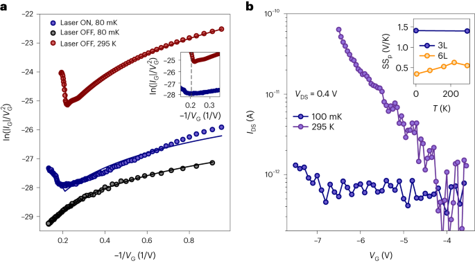
a, Tunnelling current in the 3L device without laser illumination at 100 mK (black) and 295 K (red). The logarithmic dependence in the (mathrm{ln}left(|{I}_{mathrm{G}}text{|}/{V}_{mathrm{G}}^{2}right)) scale with respect to −1/VG for VG < −1 V reveals no transition in the dark at low temperatures and a sharp transition at room temperature. In the inset, the tunnelling photocurrent at 100 mK (blue) is compared with the dark tunnelling current at room temperature, revealing a comparable trend in the Fowler–Nordheim regime (1/VG < −0.2 V and a transition voltage of around 5 V for both cases. b, Lateral p-type transport for the 3L device at 100 mK (blue) and 295 K (violet). The thermal broadening due to Fermi–Dirac scaling with temperature induces a shift in the first-detectable subthreshold p-type signal33, as further discussed in Supplementary Note 2. However, no substantial change in the subthreshold slope is detected. In the inset, the p-type subthreshold slopes (SSp) of the 3L (blue) and 6L (yellow) devices are shown. The sizeable difference in magnitude of ({mathrm{SS}}_{mathrm{p}}^{3{mathrm{L}}}) and ({mathrm{SS}}_{mathrm{p}}^{6{mathrm{L}}}) both at room and cryogenic temperatures is related to the increase in hole effective mass in InSe for a decreasing number of layers.
We further observe a change in the lateral transport of holes at low and high temperatures (Fig. 4b). In fact, the presence of in-gap defect states influences the transport characteristics, as discussed in Supplementary Note 2. Due to the high hole effective mass (Supplementary Note 1), it is difficult to identify the valence-band edge from the onset of hole conduction in thinner InSe samples (n ≤ 3L). This explains the higher discrepancy in the quantities of interest shown in Fig. 3e between 3L and thicker samples. We can conclude that, while the onset of p-type conduction in our InSe devices is affected by the presence of defect states at room temperature, the tunnelling current transition voltage remains unaffected. Such a result supports the use of tunnelling currents as a reliable mechanism to electrically detect van Hove singularities of flat-band systems in field-effect devices.
- SEO Powered Content & PR Distribution. Get Amplified Today.
- PlatoData.Network Vertical Generative Ai. Empower Yourself. Access Here.
- PlatoAiStream. Web3 Intelligence. Knowledge Amplified. Access Here.
- PlatoESG. Automotive / EVs, Carbon, CleanTech, Energy, Environment, Solar, Waste Management. Access Here.
- PlatoHealth. Biotech and Clinical Trials Intelligence. Access Here.
- ChartPrime. Elevate your Trading Game with ChartPrime. Access Here.
- BlockOffsets. Modernizing Environmental Offset Ownership. Access Here.
- Source: https://www.nature.com/articles/s41565-023-01489-x
- :has
- :is
- :not
- :where
- ][p
- 1
- 10
- 100
- 11
- 12
- 125
- 16
- 17
- 19
- 1985
- 1995
- 20
- 2011
- 2013
- 2016
- 2017
- 2018
- 2020
- 2021
- 2022
- 22
- 23
- 24
- 25
- 26
- 27
- 28
- 2D
- 30
- 33
- 39
- 46
- 50
- 7
- 8
- 80
- a
- Account
- Accounting
- accumulation
- achieved
- AIR
- AL
- allow
- allowed
- Allowing
- allows
- also
- an
- Anchor
- and
- any
- applied
- Apply
- ARE
- around
- AS
- At
- attention
- b
- back
- BAND
- bar
- barrier
- barriers
- bars
- based
- basis
- BE
- Beam
- become
- been
- Beginning
- between
- binding
- Black
- Blue
- both
- Bottom
- button
- by
- calculated
- CAN
- carriers
- case
- cases
- change
- Changes
- changing
- characteristics
- characterizes
- charge
- chow
- circles
- click
- Close
- closely
- combination
- Common
- commonly
- comparable
- compare
- compared
- complete
- conclude
- conductivity
- Consider
- consistent
- contacts
- contribution
- Corresponding
- corresponds
- crucial
- cryogenic
- Crystal
- Current
- curve
- Dark
- data
- decrease
- deep
- dense
- density
- dependence
- desire
- detected
- Detection
- device
- Devices
- diagrams
- difference
- different
- difficult
- direct
- directly
- discrepancy
- discussed
- discussion
- Dispersion
- displaying
- divided
- does
- dominant
- DOS
- due
- during
- e
- E&T
- Edge
- effect
- Effective
- effects
- either
- Electric
- Electronic
- emission
- encapsulated
- energy
- enhance
- enhanced
- ensures
- entered
- Enters
- equipped
- error
- Ether (ETH)
- EV
- example
- excited
- excluded
- exhibits
- Explain
- Explains
- exponential
- exposed
- extending
- extract
- fact
- factor
- false
- field
- Fields
- Fig
- Figure
- Film
- findings
- fitting
- five
- fixed
- flat
- Focus
- following
- For
- formation
- formed
- Former
- formula
- from
- full
- function
- functional
- further
- Gain
- gap
- generation
- Giving
- Graphene
- Hall
- Handling
- Harnessing
- Have
- heights
- hence
- here
- High
- high-quality
- higher
- highest
- Highlight
- Highlighted
- highlights
- Hole
- Holes
- HOT
- However
- hq
- HTTPS
- hundred
- Hundreds
- Hybrid
- identified
- identify
- if
- image
- in
- Increase
- increasing
- indicate
- indicates
- influencing
- initial
- input
- insights
- interactions
- interest
- into
- investigate
- IT
- ITS
- itself
- known
- laser
- layer
- layered
- layers
- Level
- levels
- lies
- light
- likely
- Line
- lines
- LINK
- literature
- located
- Low
- lower
- Main
- mainly
- Mass
- masses
- matching
- material
- materials
- mean
- measured
- measurement
- measurements
- mechanism
- mechanisms
- metal
- method
- MEV
- Microscope
- minimum
- minor
- mobility
- Moreover
- most
- motivated
- nano
- Nanophotonics
- nanotechnology
- Nature
- Near
- needed
- never
- no
- notably
- Notes
- number
- observe
- obtain
- obtained
- of
- offsets
- on
- ONE
- ones
- only
- optimization
- or
- order
- Origin
- Other
- our
- out
- over
- parameters
- part
- particular
- Peak
- perform
- performed
- Physics
- picture
- plato
- Plato Data Intelligence
- PlatoData
- Play
- plays
- Point
- position
- possibility
- power
- predicted
- predominantly
- presence
- present
- presented
- previously
- probability
- Problem
- process
- produce
- properties
- proposed
- provided
- Quantum
- R
- range
- rapid
- ratio
- reaching
- Red
- Reduced
- reduction
- regarding
- regime
- regimes
- region
- regions
- related
- relationship
- relatively
- reliable
- remains
- reminiscent
- Reported
- Reports
- represented
- representing
- resilience
- respect
- respective
- respectively
- response
- responsible
- result
- Results
- reveal
- revealing
- Reveals
- right
- Rise
- Role
- Room
- roughly
- Rule
- rules
- Scale
- scaling
- scheme
- SCI
- SEA
- Section
- sections
- seen
- semiconductor
- Semiconductors
- several
- sharp
- shift
- Shifts
- show
- shown
- Shows
- Signal
- signals
- similar
- since
- singularity
- Size
- Slope
- Source
- Spectroscopy
- stacked
- standard
- start
- State
- States
- stress
- strong
- strongly
- structure
- studies
- Study
- subject
- substantial
- successful
- Successfully
- such
- sudden
- Superconductivity
- Supports
- suppression
- surf
- Surface
- susceptible
- system
- Systems
- T
- table
- taking
- thanks
- that
- The
- their
- theory
- therefore
- thermal
- These
- this
- three
- three-dimensional
- Through
- to
- together
- too
- top
- Total
- transfer
- transition
- transport
- Transport properties
- Trend
- Trends
- true
- tunnel
- two
- type
- unaffected
- unconventional
- under
- understand
- understanding
- unveiling
- us
- use
- used
- using
- Values
- vertical
- View
- visible
- Voltage
- want
- was
- we
- WELL
- Wells
- were
- when
- which
- while
- wide
- with
- within
- without
- would
- yellow
- zephyrnet