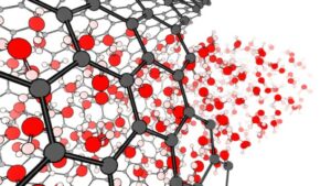

A new ultrahigh-density optical storage technology that can store up to nine bits of information per diffraction-limited area that works thanks to a deep learning approach has been put forward by researchers in Toulouse in France. The technology overcomes the physical constraints of compact disks (CDs), DVDs and Blu-ray disks, which can only store one bit per diffraction-limited area. It is based on silicon and could thus be produced on a large scale using mass-market-ready complementary metal-oxide-semiconductor (CMOS) technology.
The storage capacity of magnetic hard disk drives is reaching its limits and it will soon no longer be able to meet the demand of the increasing volumes of data being generated each day. Optical data storage is a promising alternative because it can store much higher volumes (over 10 terabytes) and for longer periods (hundreds of years compared to just five to ten years for hard disk drives).
The storage capacity of current optical data storage technologies such as the CD, DVD and Blu-ray disk is, however, restricted by the diffraction limit of the laser used to write to the disk. This means that they can store just a single bit per diffraction-limited area (“0” or “1”) to reach 200 gigabytes per disk at best. Ways to increase optical information density – such as using polarization-sensitive digits, near-field optical recording, two-photon point excitation or holographic memory – do exist but no commercial product based on these technologies is yet available.
Encoding information in subwavelength silicon nanostructures
A team of researchers from CEMES and LAAS-CNRS, both in Toulouse, has now put forward a new way to encode multiple bits of digital information in subwavelength silicon nanostructures. Thanks to the high refractive index of silicon, these nanostructures scatter light with little loss. The researchers retrieve the information stored in these particles using a machine-learning-based approach in which an artificial neuronal network (ANN) analyses their scattering spectra.
ANNs are computational schemes that can be trained to efficiently solve problems that are challenging for a classical computer, explains study lead author Peter Wiecha of CEMES. “Although ANNs have many applications – including, for example in modern smartphones or for interpreting medical images – research in nano-optics has only begun to harness the tremendous potential of machine learning.”
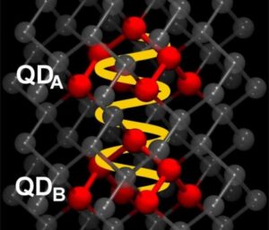
The researchers studied a 300 x 300 nm2 square of nanoparticles subdivided into smaller blocks measuring 120 x 120 nm2 that encode the information bits. “Our approach is simple,” explains Wiecha. “We made a small checker-board-like nanostructure surrounded by an asymmetric border. If a block in this nano-array is occupied by a silicon nanoparticle, then the according bit is ‘1’. If it is empty, the encoded bit is ‘0’.”
A four-bit array (four blocks) can be used to encode four bits (a “nibble” or half-byte) of information.
Reading out the encoded data
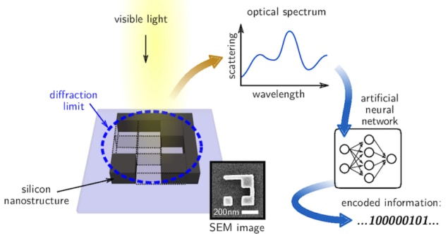
Once they had defined the nano-geometry for encoding multiple bits in the diffraction-limited area in their blocks, the researchers then needed to read out the encoded data using a simple optical set up that is robust to unavoidable structural defects in the material and instrumental noise. They did this by collecting the optical spectra of their arrays with a dark-field microscope and postprocessing these spectra with an ANN. “The asymmetric border around the checker-board nanostructure renders each pattern unique and gives it an exclusive optical scattering response when probed with polarized light in our microscope,” explains Wiecha.
“Our idea is to train a deep ANN on a large number of nanostructures and their experimentally measured scattering spectra,” he tells Physics World. “We found that it is indeed possible to read out, quasi-error-free, up to nine bits per diffraction-limited area using such a deep learning approach. And that is not all: once trained, the ANN is extremely fast.”
The researchers say that they do not even need to analyse the full spectra from the nanostructures but can accurately retrieve the information by probing just three to five specific wavelengths. “For example, the red, green and blue (RGB) spectral windows from microscopy images is all we require,” says Wiecha. “This type of analysis might be done using hand-held smartphone-microscopy (a field that has seen some important advances recently), making the technique easily accessible to all.”

Super resolution microscopy gets a dose of deep learning
Compatible with CMOS
The new work could help open the way towards high-density optical information storage using planar silicon nanostructures, says Wiecha. “Importantly, the technique we have developed is also compatible with mass-production-ready CMOS technology.
“We are now looking at how small we can make our nanostructures without introducing significant error rates, and trying to find out if we can increase the number of bits per diffraction-limited area,” he reveals.
The present research is detailed in Nature Nanotechnology.
- SEO Powered Content & PR Distribution. Get Amplified Today.
- PlatoData.Network Vertical Generative Ai. Empower Yourself. Access Here.
- PlatoAiStream. Web3 Intelligence. Knowledge Amplified. Access Here.
- PlatoESG. Automotive / EVs, Carbon, CleanTech, Energy, Environment, Solar, Waste Management. Access Here.
- PlatoHealth. Biotech and Clinical Trials Intelligence. Access Here.
- ChartPrime. Elevate your Trading Game with ChartPrime. Access Here.
- BlockOffsets. Modernizing Environmental Offset Ownership. Access Here.
- Source: https://physicsworld.com/a/deep-learning-improves-optical-storage/
- :has
- :is
- :not
- ][p
- $UP
- 10
- 200
- 300
- 90
- a
- Able
- accessible
- According
- accurately
- advances
- All
- also
- alternative
- an
- analyse
- analysis
- and
- applications
- approach
- ARE
- AREA
- around
- Array
- artificial
- AS
- At
- author
- available
- based
- BE
- because
- been
- begun
- being
- BEST
- Bit
- Block
- Blocks
- Blue
- border
- both
- but
- by
- CAN
- Capacity
- CD
- CDS
- challenging
- Collecting
- commercial
- compared
- compatible
- complementary
- computer
- constraints
- could
- Current
- data
- data storage
- day
- deep
- deep learning
- defined
- Demand
- density
- detailed
- developed
- DID
- digital
- digits
- do
- done
- dose
- drives
- DVD
- each
- easily
- efficiently
- error
- Even
- example
- Exclusive
- exist
- Explains
- extremely
- FAST
- field
- Find
- five
- For
- Forward
- found
- four
- France
- from
- full
- generated
- gives
- Green
- had
- Hard
- harness
- Have
- he
- help
- High
- higher
- holographic
- How
- However
- http
- HTTPS
- Hundreds
- idea
- if
- image
- images
- important
- improves
- in
- Including
- Increase
- increasing
- index
- information
- instrumental
- into
- introducing
- issue
- IT
- ITS
- jpg
- just
- large
- laser
- lead
- learning
- light
- LIMIT
- limits
- little
- longer
- looking
- loss
- machine
- machine learning
- made
- make
- Making
- many
- material
- max-width
- means
- measured
- measuring
- medical
- Meet
- Memory
- Microscope
- Microscopy
- might
- Modern
- much
- multiple
- Nature
- Need
- needed
- network
- neuronal
- New
- no
- Noise
- now
- number
- of
- on
- once
- ONE
- only
- open
- or
- our
- out
- over
- Pattern
- per
- periods
- physical
- Physics
- Physics World
- plato
- Plato Data Intelligence
- PlatoData
- Point
- possible
- potential
- present
- problems
- Produced
- Product
- promising
- put
- Rates
- reach
- reaching
- Read
- recently
- recording
- Red
- renders
- require
- research
- researchers
- Resolution
- response
- restricted
- Reveals
- RGB
- robust
- say
- says
- Scale
- schemes
- seen
- set
- significant
- Silicon
- Simple
- single
- small
- smaller
- smartphones
- SOLVE
- some
- Soon
- specific
- Spectral
- storage
- store
- stored
- structural
- studied
- Study
- such
- surrounded
- team
- Technologies
- Technology
- tells
- ten
- thanks
- that
- The
- the information
- their
- then
- These
- they
- this
- three
- thumbnail
- Thus
- to
- towards
- Train
- trained
- tremendous
- true
- type
- unique
- used
- using
- volumes
- wavelengths
- Way..
- ways
- we
- when
- which
- will
- windows
- with
- without
- Work
- works
- world
- write
- X
- years
- yet
- zephyrnet