News: Suppliers
6 September 2023
At the SEMICON Taiwan 2023 event in Taipei (6-8 September), deposition equipment maker Aixtron SE of Herzogenrath, near Aachen, Germany has launched its new G10-GaN cluster metal-organic chemical vapor deposition (MOCVD) platform for gallium nitride (GaN)-based power and radio frequency (RF) devices, offering what is claimed to be best-in-class performance, an all-new compact design, and overall lowest cost per wafer.
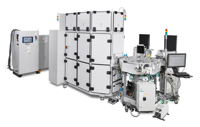 Picture: Aixtron’s new G10-GaN MOCVD system.
“Our new G10-GaN platform has already been qualified for volume production of GaN power devices by a leading US device manufacturer,” notes CEO & president Dr Felix Grawert. “The new platform delivers twice the productivity per cleanroom area than our previous product while enabling a new level of material uniformities, unlocking new levers of competitiveness for our customers,” he adds. “GaN power devices are set to play a decisive role in reducing global CO2 emissions by offering a much more efficient power conversion than conventional silicon, reducing losses by a factor of two to three. We expect this market to grow continually by the end of the decade and beyond. Today, GaN has already replaced silicon for fast chargers used in mobile devices, and we see an increasing demand for data centers or solar applications.”
Aixtron has been developing GaN-on-Si processes and hardware for more than 20 years. Its AIX G5+ C planetary reactor was the first fully automated GaN MOCVD system due to In-Situ Cleaning and Cassette-to-Cassette automation. The all-new G10-GaN cluster solution builds on the same fundamentals while extending each single performance metric.
Packed in a new, compact layout to take advantage of the smallest cleanroom space, the platform comes with novel reactor inlets, improving material uniformity by a factor of two for optimum device yields. On-board sensors are complemented by a new software suite and fingerprint solutions to ensure that the system consistently delivers the same performance run after run, between maintenance for all process modules – extending the equipment uptime by more than 5% compared with the previous generation.
The cluster can be equipped with up to three process modules, delivering a record capacity of 15x200mm wafers due to Planetary batch reactor technology – enabling a 25% cost reduction per wafer compared with previous products.
Aixtron investing up to €100m to build new innovation center
Aixtron launching G10-AsP system at Photonic West
Aixtron launches G10-SiC 200mm CVD system
- SEO Powered Content & PR Distribution. Get Amplified Today.
- PlatoData.Network Vertical Generative Ai. Empower Yourself. Access Here.
- PlatoAiStream. Web3 Intelligence. Knowledge Amplified. Access Here.
- PlatoESG. Automotive / EVs, Carbon, CleanTech, Energy, Environment, Solar, Waste Management. Access Here.
- PlatoHealth. Biotech and Clinical Trials Intelligence. Access Here.
- ChartPrime. Elevate your Trading Game with ChartPrime. Access Here.
- BlockOffsets. Modernizing Environmental Offset Ownership. Access Here.
- Source: https://www.semiconductor-today.com/news_items/2023/sep/aixtron-060923.shtml
- :has
- :is
- $UP
- 20
- 20 years
- 2023
- a
- Adds
- ADvantage
- After
- All
- already
- an
- and
- applications
- ARE
- AREA
- At
- Automated
- Automation
- BE
- been
- between
- Beyond
- build
- builds
- by
- CAN
- Capacity
- Centers
- ceo
- chemical
- claimed
- Cleaning
- Cluster
- comes
- compact
- compared
- competitiveness
- consistently
- continually
- conventional
- Conversion
- Cost
- cost reduction
- Customers
- data
- data centers
- decade
- decisive
- delivering
- delivers
- Demand
- Design
- developing
- device
- Devices
- dr
- due
- each
- efficient
- Emissions
- enabling
- end
- ensure
- equipment
- equipped
- Ether (ETH)
- Event
- expect
- extending
- factor
- FAST
- fingerprint
- First
- For
- Frequency
- fully
- Fundamentals
- generation
- Germany
- Global
- Grow
- Hardware
- he
- http
- HTTPS
- improving
- in
- increasing
- Innovation
- investing
- items
- ITS
- jpg
- launched
- launches
- launching
- Layout
- leading
- Level
- losses
- lowest
- maintenance
- maker
- Manufacturer
- Market
- material
- metric
- Mobile
- mobile devices
- Modules
- more
- more efficient
- much
- Near
- New
- New Platform
- Notes
- novel
- of
- offering
- on
- optimum
- or
- our
- overall
- per
- performance
- platform
- plato
- Plato Data Intelligence
- PlatoData
- Play
- power
- president
- previous
- process
- processes
- Product
- Production
- productivity
- Products
- qualified
- Radio
- reactor
- record
- reducing
- reduction
- related
- replaced
- Role
- Run
- same
- see
- sensors
- September
- set
- Silicon
- single
- Software
- solar
- solution
- Solutions
- Space
- suite
- system
- Taiwan
- Take
- Technology
- than
- that
- The
- this
- three
- to
- today
- Twice
- two
- unlocking
- uptime
- us
- used
- volume
- was
- we
- What
- What is
- while
- with
- years
- yields
- zephyrnet