We have been working with Keysight EDA for the past two years and it has been an honor. The technical depth we have reached with them is impressive. Niels Faché, VP & GM, Keysight EDA, is responsible for Keysight’s design and simulation portfolio. Niels has been part of the Keysight-Agilent-HP family since 1994 when HP acquired Alphabit, a company he co-founded.
Tell us a little bit about Keysight EDA.
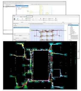
Keysight EDA is the design and simulation business inside Keysight Technologies test and measurement business. Our EDA solutions are focused on high speed, high frequency design problems. They include RF and microwave circuit and system design for MMICs and RFICs and modules, phased arrays, wireless and satellite systems, high-speed digital design for signal integrity, power integrity of complex modules and boards, memory and interconnect design, semiconductor device modeling, and power electronics, and of course process and data management (Cliosoft).
What was the most exciting high point of 2023 for your company?
The acquisition of Cliosoft in the design data and IP management space. Progress on partnerships with Synopsys, Ansys, Altium, and TSMC, Samsung on the foundry side. Introduction of new capabilities in our software suite that support mmWave workflows, Python automation, AI/ML in device modeling and more.
What was the biggest challenge your company faced in 2023?
Being recognized as a top-tier rather than niche EDA industry player. We made headway on this with our involvement in the ESD Alliance and showing at DAC.
How is your company’s work addressing this biggest challenge?
We are broadening our product portfolio to appeal to a larger audience. We are addressing customer pain points with design complexity and time to market requirements by focusing on connected design and test workflows and shift left from physical to virtual prototypes where issues can be resolved earlier and more cost effectively.
What do you think the biggest growth area for 2024 will be, and why?
In 2024, engineers will continue embracing shift left with their electronic product development cycles. As design moves from the physical into the virtual space, engineers are able to quickly discover and fix problems in the most efficient manner, providing greater insights and performance improvements. The next few years will see a continuing emphasis on connecting design and test workflows to handle rising complexity and more demanding time-to-market requirements for electronic products in wireless, wired, aerospace/defense, and other industries. Here are the emerging electronic design innovations we see for 2024:
3DIC and Heterogeneous Chiplets: New Standards Come into View
New standards such as UCIe are emerging for the creation of chiplets and the disaggregation of system-on-chip designs into smaller pieces of intellectual property that can be assembled into 2.5D and 3D integrated circuits using advanced packaging. For designers to accurately simulate die-to-die physical layer interconnect, it will require high-speed, high-frequency channel simulation to UCIe and other standards.
EDA Turns to AI: From Complexity to Clarity
The application of AI and ML techniques in EDA is still in the early adopter phase, with design engineers exploring use cases to simplify complex problems. The intelligence is particularly valuable in model development and validation for simulation, where it assists in processing large volumes of data. In 2024, organizations will increasingly adopt both technologies for device modeling of silicon and III-V semiconductor process technologies, as well as system modeling for forthcoming standards such as 6G, where research is well underway.
Software Automation Empowers Engineers
As Moore’s Law reaches its limits, improving design processes through workflow automation will provide a pathway to increasing the productivity of design engineers. In 2024, software automation techniques, such as Python APIs, will take a more significant role in integrating “best-in-class” tools into open, interoperable design and test ecosystems.
Navigating the Digital Shift: Design Management Essentials
With the creation of digital enterprise workflows, many organizations are investing in design management across tool sets, data, and IP. Moving forward, design data and IP management software will play a critical role in the success of complex SoC and heterogeneous chiplet designs supporting large, geographically distributed teams. Creation of digital threads between requirements definition and compliance, and establishing tighter links with enterprise systems such as PLM also play a role in digital transformation of product development cycles.
Next-Gen Quantum Design: Optimizing System Performance
Quantum computing is advancing at a rapid pace and is transitioning from predominantly free research tools to commercial products and workflows in quantum design. Next-generation quantum design will require more integrated simulation workflows that provide developers with fast and accurate capabilities to optimize system performance.
Silicon Photonics Fuels Data Center Transformation
Data centers are evolving to provide higher compute performance to support the exponential growth in AI and ML workloads, as well as the need for more efficient power utilization and thermal management. Silicon photonics will play a critical role in accelerating the transformation of data centers to meet the appetite for compute performance. As design engineers develop high-speed data center chips that incorporate silicon photonics interconnect, they will need process design kits (PDKs) and accurate simulation models that support the advanced development work.
How is your company’s work addressing this growth?
We work closely with customers to solve their design, simulation, and workflow problems. We focus on growth sub-segments of the market and are seeing strong growth in our high-speed digital business. We are launching new simulation engines and workflows, for example focused on UCIe simulation for chiplets. We incorporate measurement science into our products to make them more accurate.
What conferences did you attend in 2023 and how was the traffic?
DesignCon, OFC, TSMC Tech Symposium and OIP Forum, DAC, IMS, European Microwave Week and others. DAC was the highlight for us last year. We had a very strong presence with many customer meetings. It was a big success leveraging Cliosoft’s past approach to DAC for Keysight EDA. Our EDA business is relationship driven and we value show participation as a way to foster those relationships and initiate new relationships. We will be participating in the same conferences this year in addition to the Chiplet Summit and SNUG.
Also Read:
Higher-order QAM and smarter workflows in VSA 2023
Advanced EM simulations target conducted EMI and transients
Seeing 1/f noise more accurately
Share this post via:- SEO Powered Content & PR Distribution. Get Amplified Today.
- PlatoData.Network Vertical Generative Ai. Empower Yourself. Access Here.
- PlatoAiStream. Web3 Intelligence. Knowledge Amplified. Access Here.
- PlatoESG. Carbon, CleanTech, Energy, Environment, Solar, Waste Management. Access Here.
- PlatoHealth. Biotech and Clinical Trials Intelligence. Access Here.
- Source: https://semiwiki.com/eda/keysight-eda/341215-2024-outlook-with-niels-fache-of-keysight-eda/
- :has
- :is
- :where
- 1994
- 2%
- 2023
- 2024
- 220
- 3d
- 6G
- a
- Able
- About
- accelerating
- accurate
- accurately
- acquired
- acquisition
- across
- addition
- addressing
- adopt
- advanced
- advancing
- AI
- AI/ML
- Alliance
- also
- an
- and
- APIs
- appeal
- appetite
- Application
- approach
- ARE
- AREA
- AS
- assembled
- assists
- At
- attend
- audience
- Automation
- BE
- been
- between
- Big
- Biggest
- Bit
- both
- business
- by
- CAN
- capabilities
- cases
- Center
- Centers
- challenge
- Channel
- Chips
- circuit
- circuits
- closely
- come
- commercial
- company
- Company’s
- complex
- complexity
- compliance
- Compute
- computing
- conducted
- conferences
- connected
- Connecting
- continue
- continuing
- Cost
- course
- creation
- critical
- customer
- Customers
- cycles
- data
- Data Center
- data centers
- data management
- definition
- demanding
- depth
- Design
- designers
- designs
- develop
- developers
- Development
- device
- DID
- digital
- Digital Transformation
- discover
- distributed
- do
- driven
- Earlier
- Early
- Ecosystems
- effectively
- efficient
- Electronic
- Electronics
- embracing
- emerging
- emphasis
- empowers
- Engineers
- Engines
- Enterprise
- establishing
- Ether (ETH)
- European
- Event
- evolving
- example
- exciting
- Exploring
- exponential
- Exponential Growth
- faced
- family
- FAST
- few
- Fix
- Focus
- focused
- focusing
- For
- forthcoming
- Forum
- Forward
- Foster
- Foundry
- Free
- Frequency
- from
- fuels
- geographically
- GM
- greater
- Growth
- growth area
- had
- handle
- Have
- he
- here
- High
- High-Frequency
- higher
- Highlight
- honor
- How
- HP
- HTTPS
- impressive
- improvements
- improving
- in
- include
- incorporate
- increasing
- increasingly
- industries
- industry
- initiate
- innovations
- inside
- insights
- integrated
- Integrating
- integrity
- intellectual
- intellectual property
- Intelligence
- interoperable
- into
- Introduction
- investing
- involvement
- IP
- issues
- IT
- ITS
- jpg
- large
- larger
- Last
- Last Year
- launching
- Law
- layer
- left
- leveraging
- limits
- links
- little
- made
- make
- management
- manner
- many
- Market
- max-width
- measurement
- Meet
- meetings
- Memory
- ML
- ML techniques
- model
- modeling
- models
- Modules
- more
- more efficient
- most
- moves
- moving
- Need
- New
- next
- next-generation
- niche
- Noise
- of
- on
- open
- Optimize
- optimizing
- organizations
- Other
- Others
- our
- Outlook
- Pace
- packaging
- Pain
- Pain points
- part
- participating
- participation
- particularly
- partnerships
- past
- pathway
- performance
- phase
- Phased
- physical
- pieces
- plato
- Plato Data Intelligence
- PlatoData
- Play
- player
- Point
- points
- portfolio
- Post
- power
- predominantly
- presence
- problems
- process
- processes
- processing
- Product
- product development
- productivity
- Products
- Progress
- property
- prototypes
- provide
- providing
- Python
- Quantum
- quickly
- rapid
- rather
- reached
- Reaches
- Read
- recognized
- relationship
- Relationships
- require
- Requirements
- research
- resolved
- responsible
- rising
- Role
- same
- Samsung
- satellite
- Science
- see
- seeing
- semiconductor
- Sets
- shift
- show
- showing
- side
- Signal
- significant
- Silicon
- simplify
- simulate
- simulation
- simulations
- since
- smaller
- smarter
- Software
- Solutions
- SOLVE
- Space
- speed
- standards
- Still
- strong
- success
- such
- suite
- support
- Supporting
- Symposium
- system
- Systems
- Take
- Target
- teams
- tech
- Technical
- techniques
- Technologies
- test
- than
- that
- The
- their
- Them
- thermal
- they
- think
- this
- this year
- those
- Through
- tighter
- time
- to
- tool
- tools
- traffic
- Transformation
- transitioning
- Tsmc
- turns
- two
- Underway
- us
- use
- using
- validation
- Valuable
- value
- very
- via
- Virtual
- Virtual space
- volumes
- vp
- was
- Way..
- we
- week
- WELL
- when
- why
- will
- wireless
- with
- Work
- workflow
- workflow automation
- workflows
- working
- year
- years
- you
- Your
- zephyrnet