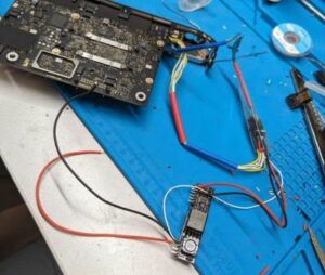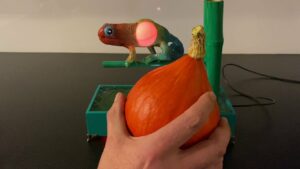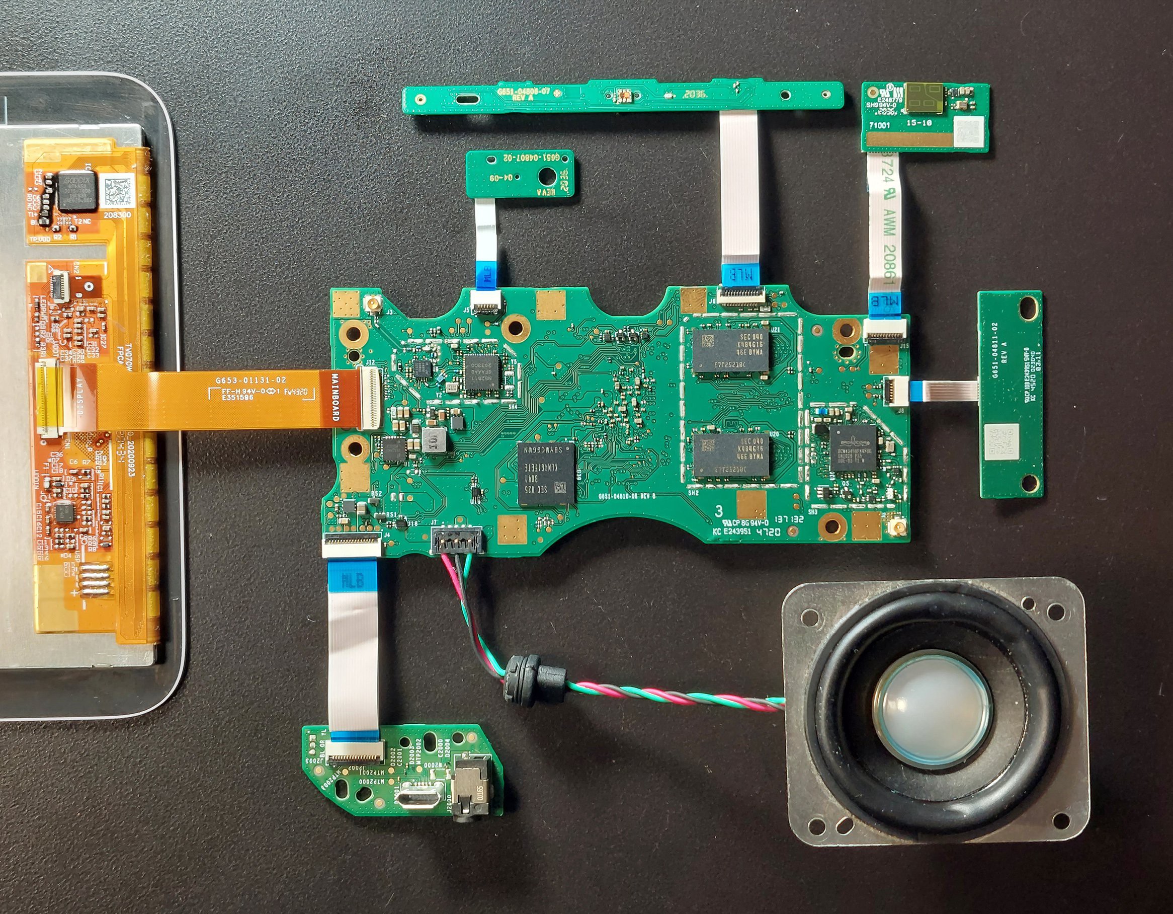
Seeing the guts of devices is a fascination that many hackers share. [Txyz] tore down a 2nd gen Google Nest Hub for all of us to enjoy. The video after the break is well produced and relaxing to watch as various heat shields are removed and debug cables are soldered on.
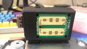
The main SOC is an Amlogic S905D3G, a 4-core A55-based SoC. The important chips are meticulously documented, and it’s a fascinating look inside a device common in many people’s homes. One chip that’s of note is the BGT60TR13C, otherwise known as Project Soli. It is an 8x10mm chip that uses radar to detect movement with sub-millimeter accuracy. This allows the device to measure your sleep quality or recognize gestures. Luckily for us, [Txyz] has included a datasheet and a block diagram. First, the chip fills a FIFO with data samples. Once full, it will issue an interrupt to the main SoC, which empties the buffer via SPI.
The debug cables allowed him to capture traces of the SPI commands to the BGT60TR13C. [Txyz] focused on decoding the various data blocks and the configuration registers. Unfortunately, only a few registers are documented in the datasheet, and it isn’t apparent what they do.
If a hardware teardown isn’t enough for you, perhaps a software teardown to bypass Secure Boot might sate your interest.
- SEO 기반 콘텐츠 및 PR 배포. 오늘 증폭하십시오.
- PlatoAiStream. Web3 데이터 인텔리전스. 지식 증폭. 여기에서 액세스하십시오.
- 미래 만들기 w Adryenn Ashley. 여기에서 액세스하십시오.
- PREIPO®로 PRE-IPO 회사의 주식을 사고 팔 수 있습니다. 여기에서 액세스하십시오.
- 출처: https://hackaday.com/2023/05/29/google-nest-hub-teardown/