WASHINGTON — The Defense Department moved to establish eight regional microelectronics hubs in seven states across the U.S., aimed at helping spur manufacturing innovation to bolster the domestic semiconductor industrial base.
Defense Secretary Kathleen Hicks told reporters during a Sept. 20 Pentagon briefing the awards total $238 million with each innovation hub receiving between $15 million and $40 million to establish initial operations.
XNUMX つのハブの本拠地は次のとおりです。
- New York, led by the State University of New York Polytechnic Institute;
- Arizona, led by Arizona State University;
- North Carolina, led by North Carolina State University;
- Indiana, led by the Applied Research Institute;
- Ohio, led by the Midwest Microelectronics Consortium;
- 南カリフォルニア大学が主導する南カリフォルニア。
- Northern California, led by Stanford and the University of California Berkley; and
- マサチューセッツ州、マサチューセッツ技術協力社が主導。
“The regional hubs will spur economic growth, not just locally, but more broadly,” Hicks said. “The hubs will help ensure we have the talent pool needed to stay ahead, through education pipelines and retraining initiatives. And it’s part of how DoD is reducing our reliance on foreign components, keeping us safe from the risks of supply chain disruption.”
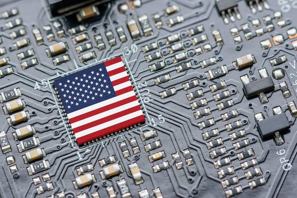
過去 30 年間で、米国は世界のマイクロチップ供給量の 37% から約 12% まで生産しました。現在、台湾は世界の先端半導体供給の大部分を生産しており、中国はマイクロチップの大部分を米国に輸出している。これらのチップ 携帯電話から自動車まであらゆるものに電力を供給 F-35戦闘機まで。
に help address domestic microelectronics supply chain vulnerabilities, Congress last year passed the Creating Helpful Incentives to Produce Semiconductors, or CHIPS ACT, providing $52 billion to fund semiconductor workforce improvement efforts, research and development and manufacturing through 2026.
The Defense Department received $2 billion in CHIPS Act funding, which it is using to establish the commons. The department expects to spend about $400 million annually through 2026 to equip the hubs and execute various technology projects focused in six areas: electronic warfare, quantum, security at the edge, internet of things, 5G and 6G and dual-use capabilities.
The Pentagon envisions the Microelectronics Commons as a 学術機関、中小企業、研究機関の全国ネットワーク 協力して、マイクロエレクトロニクス技術プロジェクトを研究室からプロトタイピングと大規模生産へと推し進めます。
The network will be made up of “cores,” or chip foundries, that provide access to prototyping and help reduce technology integration risk. The innovation hubs announced this week will help connect research projects to those regional foundries.
正式なハブの発表に先立って記者団に語った国防高官によると、国防省はXNUMX月に初のマイクロエレクトロニクス・コモンズ会議を開催し、その後、最初のプロジェクト募集を行う予定だという。イノベーションハブのリーダーに選ばれなかった組織にも、それらのプロジェクトをめぐって競争するチャンスが与えられる。
“The projects that come through will be a mix of very near term and slightly longer term,” the official told reporters in a Sept. 19 briefing. “The outcome of a successful project will be something that can be taken to scale in a U.S. based foundry.”
Courtney Albon は、C4ISRNET の宇宙および新興技術のレポーターです。 彼女は 2012 年から空軍と宇宙軍を中心に米軍を取材してきました。 彼女は、国防総省の最も重要な買収、予算、および政策上の課題のいくつかについて報告しています。
- SEO を活用したコンテンツと PR 配信。 今日増幅されます。
- PlatoData.Network 垂直生成 Ai。 自分自身に力を与えましょう。 こちらからアクセスしてください。
- プラトアイストリーム。 Web3 インテリジェンス。 知識増幅。 こちらからアクセスしてください。
- プラトンESG。 カーボン、 クリーンテック、 エネルギー、 環境、 太陽、 廃棄物管理。 こちらからアクセスしてください。
- プラトンヘルス。 バイオテクノロジーと臨床試験のインテリジェンス。 こちらからアクセスしてください。
- 情報源: https://www.defensenews.com/battlefield-tech/2023/09/20/pentagon-eyes-microelectronics-hubs-across-us-to-bolster-chip-industry/
- :持っている
- :は
- :not
- 400 億円
- $UP
- 10
- 19
- 20
- 2012
- 2026
- 30
- 5G
- 6G
- 70
- a
- 私たちについて
- アカデミック
- アクセス
- 従った
- 買収
- 越えて
- 行為
- 住所
- 高度な
- 後
- 先んじて
- 目的としました
- 空気
- 空軍
- および
- 発表の
- お知らせ
- 年単位
- 適用された
- です
- エリア
- アリゾナ州
- アリゾナ州立大学
- 周りに
- AS
- At
- 賞を受賞
- ベース
- BE
- の間に
- 10億
- ボルスター
- ブリーフィング
- 広く
- 予算
- ビジネス
- 焙煎が極度に未発達や過発達のコーヒーにて、クロロゲン酸の味わいへの影響は強くなり、金属を思わせる味わいと乾いたマウスフィールを感じさせます。
- by
- カリフォルニア州
- コール
- 缶
- 機能
- カロライナ
- セル
- 携帯電話
- チェーン
- 課題
- チャンス
- 中国
- チップ
- チップ
- チップ法
- 共同
- 来ます
- コモンズ
- 競争する
- コンポーネント
- 議会
- お問合せ
- コンソーシアム
- カバー
- 作成
- CTO
- 防衛
- 国防省
- 部門
- 開発
- 途絶
- DoD
- 国内の
- 間に
- 各
- 経済
- 経済成長
- エッジ(Edge)
- 教育
- 努力
- エレクトロニック
- 新興の
- 新興テクノロジー
- 確保
- 構想する
- 確立する
- すべてのもの
- 実行します
- 期待する
- 輸出
- 視線
- 企業
- 名
- フォーカス
- 焦点を当て
- 強
- 外国の
- フォーマル
- ファウンドリ
- から
- ファンド
- 資金調達
- グローバル
- 行って
- 成長性
- 持ってる
- 助けます
- 役立つ
- 助け
- ホーム
- 認定条件
- HTTPS
- ハブ
- ハブ
- 画像
- 改善
- in
- インセンティブ
- インダストリアル
- 産業を変えます
- 初期
- イニシアチブ
- 革新的手法
- イノベーションハブ
- 機関
- 機関
- 統合
- インターネット
- モノのインターネット
- に
- 問題
- IT
- ITS
- JPG
- ただ
- 保管
- 実験室
- 大
- 姓
- 昨年
- つながる
- ツェッペリン
- 局部的に
- より長いです
- 製
- 製造業
- マサチューセッツ州
- ご相談
- 中西部
- ミリタリー用(軍用)機材
- 百万
- ミックス
- 他には?
- 最も
- 移動
- 近く
- 必要とされる
- ネットワーク
- 新作
- ニューヨーク
- ノース
- ノースキャロライナ
- 10月
- of
- 公式
- on
- 業務執行統括
- or
- 組織
- 私たちの
- 結果
- 部
- 渡された
- 五角形
- 携帯電話
- プラトン
- プラトンデータインテリジェンス
- プラトデータ
- 方針
- プール
- 事前の
- 作り出す
- 生産する
- 作成
- 生産
- プロジェクト
- プロジェクト(実績作品)
- プロトタイピング
- 提供します
- 提供
- プッシュ
- 量子
- 受け
- 受け入れ
- 減らします
- 縮小
- 地域の
- 依存
- 報告
- レポーター
- 研究
- 研究開発
- 再訓練
- リスク
- リスク
- s
- 安全な
- 前記
- 規模
- 秘書
- セキュリティ
- 選択
- 半導体
- 半導体関連装置
- シニア
- セブン
- セブン
- 彼女
- 重要
- から
- SIX
- 小さい
- 中小企業
- 一部
- 何か
- 南部の
- スペース
- 宇宙軍
- 過ごす
- スタンフォード
- 都道府県
- 米国
- 滞在
- 成功した
- 供給
- サプライチェーン
- 台湾
- 撮影
- 才能
- テクノロジー
- 期間
- それ
- ステート
- ボーマン
- 物事
- この
- 今週
- それらの
- 介して
- 〜へ
- 今日
- 一緒に
- 言われ
- トータル
- 私達
- ユナイテッド
- 米国
- 大学
- カリフォルニア大学
- サザンカリフォルニア大学
- us
- さまざまな
- 非常に
- we
- 週間
- which
- 誰
- 意志
- 労働人口
- ワーキング
- 世界の
- 年
- 年
- ヨーク
- ゼファーネット