24. január 2024.
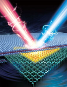
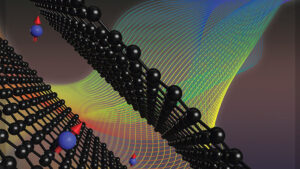
(Nanowerk News) Researchers with the Department of Energy’s SLAC National Accelerator Laboratory, Stanford University and the DOE’s Lawrence Berkeley National Laboratory (LBNL) grew a twisted multilayer crystal structure for the first time and measured the structure’s key properties. The twisted structure could help researchers develop next-generation materials for solar cells, quantum computers, lasers and other devices.
“This structure is something that we have not seen before – it was a huge surprise to me,” said Yi Cui, a professor at Stanford and SLAC and paper co-author. “A new quantum electronic property could appear within this three-layer twisted structure in future experiments.”
 FELIRAT
Rétegek hozzáadása, egy csavarral
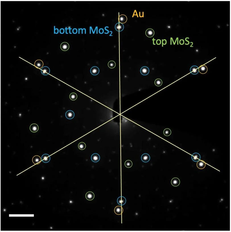
The crystals the team designed extended the concept of epitaxy, a phenomenon that occurs when one type of crystal material grows on top of another material in an ordered way – kind of like growing a neat lawn on top of soil, but at the atomic level. Understanding epitaxial growth has been critical to the development of many industries for more than 50 years, particularly the semiconductor industry. Indeed, epitaxy is part of many of the electronic devices that we use today, from cell phones to computers to solar panels, allowing electricity to flow, and not flow, through them. To date, epitaxy research has focused on growing one layer of material onto another, and the two materials have the same crystal orientation at the interface. This approach has been successful for decades in many applications, such as transistors, light-emitting diodes, lasers and quantum devices. But to find new materials that perform even better for more demanding needs, like quantum computing, researchers are searching for other epitaxial designs – ones that might be more complex, yet better performing, hence the “twisted epitaxy” concept demonstrated in this study. In their experiment, detailed in Tudomány (“Twisted epitaxy of gold nanodisks grown between twisted substrate layers of molybdenum disulfide”) a kutatók egy aranyréteget helyeztek el egy hagyományos félvezető anyag, a molibdén-diszulfid (MoS) két lapja közé.2). Because the top and bottom sheets were oriented differently, the gold atoms could not align with both simultaneously, which allowed the Au structure to twist, said Yi Cui, Professor Cui’s graduate student in materials science and engineering at Stanford and co-author of the paper. “With only a bottom MoS2 réteg, az arany szívesen igazodik hozzá, így nem történik csavar” – mondta Cui, a végzős hallgató. „De két csavart MoS-vel2 lapok, az arany nem biztos, hogy igazodik a felső vagy az alsó réteghez. Sikerült segítenünk az aranynak megoldani a zavarát, és felfedeztük az összefüggést az Au orientációja és a kétrétegű MoS csavarodási szöge között2. "Zapping arany nanolemezek
Az aranyréteg részletes tanulmányozása érdekében a Stanford Institute for Materials and Energy Sciences (SIMES) és az LBNL kutatócsoportja a teljes szerkezet mintáját 500 Celsius-fokra melegítette. Ezután a transzmissziós elektronmikroszkópiával (TEM) elnevezett technikával elektronáramot küldtek át a mintán, amely feltárta az arany nanokorongok morfológiáját, orientációját és törzsét a különböző hőmérsékleteken végzett lágyítás után. Az arany nanolemezek tulajdonságainak mérése az első szükséges lépés volt afelé, hogy megértsük, hogyan lehet az új szerkezetet a jövőben valós alkalmazásokhoz tervezni. "E tanulmány nélkül nem tudnánk, hogy egy epitaxiális fémréteget egy félvezető tetejére csavarni is lehetne" - mondta Cui, a végzős hallgató. "A teljes háromrétegű szerkezet elektronmikroszkópos mérése megerősítette, hogy ez nem csak lehetséges, hanem az is, hogy az új szerkezetet izgalmas módon lehet irányítani." Ezután a kutatók tovább szeretnék tanulmányozni az arany nanolemezek optikai tulajdonságait a TEM segítségével, és megtudni, hogy a kialakításuk megváltoztatja-e a fizikai tulajdonságokat, például az Au szalagszerkezetét. Ezt a koncepciót ki akarják terjeszteni arra is, hogy megpróbáljanak háromrétegű szerkezeteket építeni más félvezető anyagokkal és más fémekkel. „Kezdjük azt vizsgálni, hogy csak az anyagok ezen kombinációja teszi-e lehetővé ezt, vagy ez szélesebb körben is megtörténik” – mondta Bob Sinclair, a Charles M. Pigott professzora a Stanfordi Anyagtudományi és Mérnöki Iskolában, valamint a papír társszerzője. „Ez a felfedezés egy teljesen új kísérletsorozatot nyit meg, amelyet kipróbálhatunk. Úton lehetünk afelé, hogy vadonatúj anyagtulajdonságokat találjunk, amelyeket ki tudjuk használni.”- SEO által támogatott tartalom és PR terjesztés. Erősödjön még ma.
- PlatoData.Network Vertical Generative Ai. Erősítse meg magát. Hozzáférés itt.
- PlatoAiStream. Web3 Intelligence. Felerősített tudás. Hozzáférés itt.
- PlatoESG. Carbon, CleanTech, Energia, Környezet, Nap, Hulladékgazdálkodás. Hozzáférés itt.
- PlatoHealth. Biotechnológiai és klinikai vizsgálatok intelligencia. Hozzáférés itt.
- Forrás: https://www.nanowerk.com/nanotechnology-news3/newsid=64500.php
- :van
- :is
- :nem
- 10
- 13
- 14
- 24
- 50
- 50 éve
- 500
- 7
- 8
- 9
- a
- gázpedál
- hozzá
- hozzáadott
- Után
- összehangolása
- megengedett
- lehetővé téve
- lehetővé teszi, hogy
- Is
- an
- és a
- Másik
- megjelenik
- alkalmazások
- megközelítés
- VANNAK
- AS
- At
- atom
- ZENEKAR
- BE
- mert
- óta
- előtt
- Kezdet
- Berkeley
- Jobb
- között
- gabona
- mindkét
- Alsó
- márka
- Brand New
- nagyjából
- épít
- de
- hívott
- TUD
- sejt
- mobiltelefonok
- Cellák
- Celsius
- Központ
- Károly
- Társszerző
- kombináció
- teljes
- bonyolult
- számítógépek
- számítástechnika
- koncepció
- MEGERŐSÍTETT
- zavar
- vezérelt
- tudott
- kritikai
- Kristály
- találka
- évtizedek
- igényes
- igazolták
- osztály
- Design
- tervezett
- tervek
- részlet
- részletes
- Fejleszt
- Fejlesztés
- Eszközök
- különböző
- eltérően
- felfedezett
- felfedezés
- DOE
- villamos energia
- Elektronikus
- elektronok
- energia
- Mérnöki
- Még
- izgalmas
- kísérlet
- kísérletek
- Exploit
- feltárása
- terjed
- kiterjedt
- Találjon
- megtalálása
- vezetéknév
- első
- áramlási
- összpontosított
- A
- ból ből
- további
- jövő
- Arany
- diplomás
- nőtt
- Növekvő
- felnőtt
- növekszik
- Növekedés
- megtörténik
- boldog
- Legyen
- segít
- ennélfogva
- Hogyan
- HTTPS
- hatalmas
- if
- kép
- in
- iparágak
- ipar
- Intézet
- Felület
- IT
- ITS
- jpg
- Kulcs
- Kedves
- Ismer
- laboratórium
- lézerek
- Lawrence
- réteg
- tojók
- TANUL
- szint
- mint
- sikerült
- sok
- anyag
- Anyagtervezés
- anyagok
- me
- megmért
- mérő
- fém
- Fémek
- Mikroszkópia
- Középső
- esetleg
- több
- nemzeti
- Tiszta
- elengedhetetlen
- igények
- Új
- következő
- következő generációs
- nem
- of
- on
- ONE
- azok
- csak
- nyitás
- or
- Más
- mi
- panelek
- Papír
- rész
- különösen
- teljesít
- előadó
- jelenség
- telefonok
- fizikai
- Plató
- Platón adatintelligencia
- PlatoData
- lehetséges
- Egyetemi tanár
- ingatlanait
- ingatlan
- Kvantum
- kvantum számítógépek
- kvantumszámítás
- igazi
- való Világ
- kapcsolat
- kutatás
- kutató
- kutatók
- Revealed
- s
- Mondott
- azonos
- Iskola
- Tudomány
- TUDOMÁNYOK
- keres
- látott
- félvezető
- küldött
- Series of
- lap
- egyszerre
- So
- talaj
- nap
- Napelemek
- napelemek
- SOLVE
- valami
- Stanford
- Stanford Egyetem
- Lépés
- folyam
- struktúra
- struktúrák
- diák
- Tanulmány
- sikeres
- ilyen
- biztos
- meglepetés
- csapat
- technika
- szöveg
- mint
- hogy
- A
- A jövő
- azok
- Őket
- akkor
- Ezek
- ők
- ezt
- Keresztül
- idő
- nak nek
- Ma
- felső
- felé
- hagyományos
- megpróbál
- csavar
- kettő
- típus
- megértés
- egyetemi
- használ
- segítségével
- akar
- volt
- Út..
- módon
- we
- voltak
- amikor
- vajon
- ami
- egész
- val vel
- belül
- világ
- lenne
- év
- még
- zephyrnet
Még több Nanowerk
Az új rendszer gyorsan és olcsón képes észlelni a levegőben terjedő vírusokat
Forrás csomópont: 2805885
Időbélyeg: 4. augusztus 2023.
Atomléptékű spin-optikai lézer: az optoelektronikai eszközök új horizontja
Forrás csomópont: 2808400
Időbélyeg: 7. augusztus 2023.
Ultrakis örvénylő mágneses örvények észlelhetők vastartalmú anyagban
Forrás csomópont: 2559197
Időbélyeg: 2. április 2023.
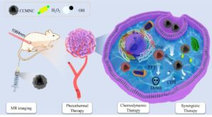
Szénbevonatú magnetit nanoklaszterek használata szinergikus rákterápiában
Forrás csomópont: 1967371
Időbélyeg: 18. február 2023.
Új kísérleti módszerrel a kutatók először vizsgálják meg a spinszerkezetet 2D anyagokban
Forrás csomópont: 2644734
Időbélyeg: May 11, 2023
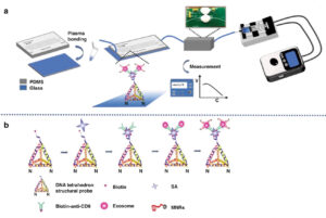
Fejlett mikrofluidikus rendszer a rák korai felismeréséhez
Forrás csomópont: 3027012
Időbélyeg: 19. december 2023.
A kutatók a bór-nitrid alapú nanokompozitok váratlan tulajdonságait fedezték fel
Forrás csomópont: 2808402
Időbélyeg: 7. augusztus 2023.
A finoman hangolt kvantumpontok javítják a nemlineáris optikát
Forrás csomópont: 1949685
Időbélyeg: 10. február 2023.
A termeszdombok felfedik a kevesebb energiát használó „élő és lélegző” épületek létrehozásának titkát
Forrás csomópont: 2680880
Időbélyeg: May 26, 2023
A váratlan kémia felfedi a kozmikus csillaggyárak titkait
Forrás csomópont: 3013622
Időbélyeg: 14. december 2023.
Nyújtható, nagy felbontású felhasználói interaktív szinesztéziás kijelző a vizuális-akusztikus titkosításhoz
Forrás csomópont: 2931119
Időbélyeg: 12. október 2023.