Copper’s resistivity depends on its crystal structure, void volume, grain boundaries and material interface mismatch, which becomes more significant at smaller scales. The formation of copper (Cu) wires is traditionally done by etching a trench pattern in low-k silicon dioxide using a trench etch process, and subsequently filling the trench with Cu via a damascene flow. Unfortunately, this method produces multi-crystalline structures with significant grain boundaries and voids, which increases the Cu wire resistance. A highly resistive TaN liner material is also utilized in this process to prevent Cu diffusion during the damascene annealing process.
Physical vapor deposition (PVD) can be used to deposit copper at high kinetic energies (between 10 to 100 eV), forming low resistance, dense single crystal structures. A drawback to PVD is that PVD deposition has a line of sight spread and can only be deposited uniformly on flat surfaces. It cannot be used to fill deep holes or trenches (figure 1a). To form isolated wire shapes, a uniform Cu layer must be deposited on a flat surface and then physically etched by ion beams. Cu forms no volatile compounds with reactive gases, so a reactive ion etch process cannot be used. Accelerated Ar ions created during ion beam etch (IBE) can remove Cu if the incident angle is very high. Unfortunately, the etchable regions will be limited due to mask shadowing effects. Figure 1b shows the regions (in red) where material cannot be etched when the mask is perpendicular to the incoming ion beam. This etch failure occurs due to either shadowing or blockage of the path of the ejected atom. When the mask is parallel to the path of the ion, all unmasked regions can be etched. Thus, ion beam etching is limited to etching line shaped masks of arbitrarily long lengths.

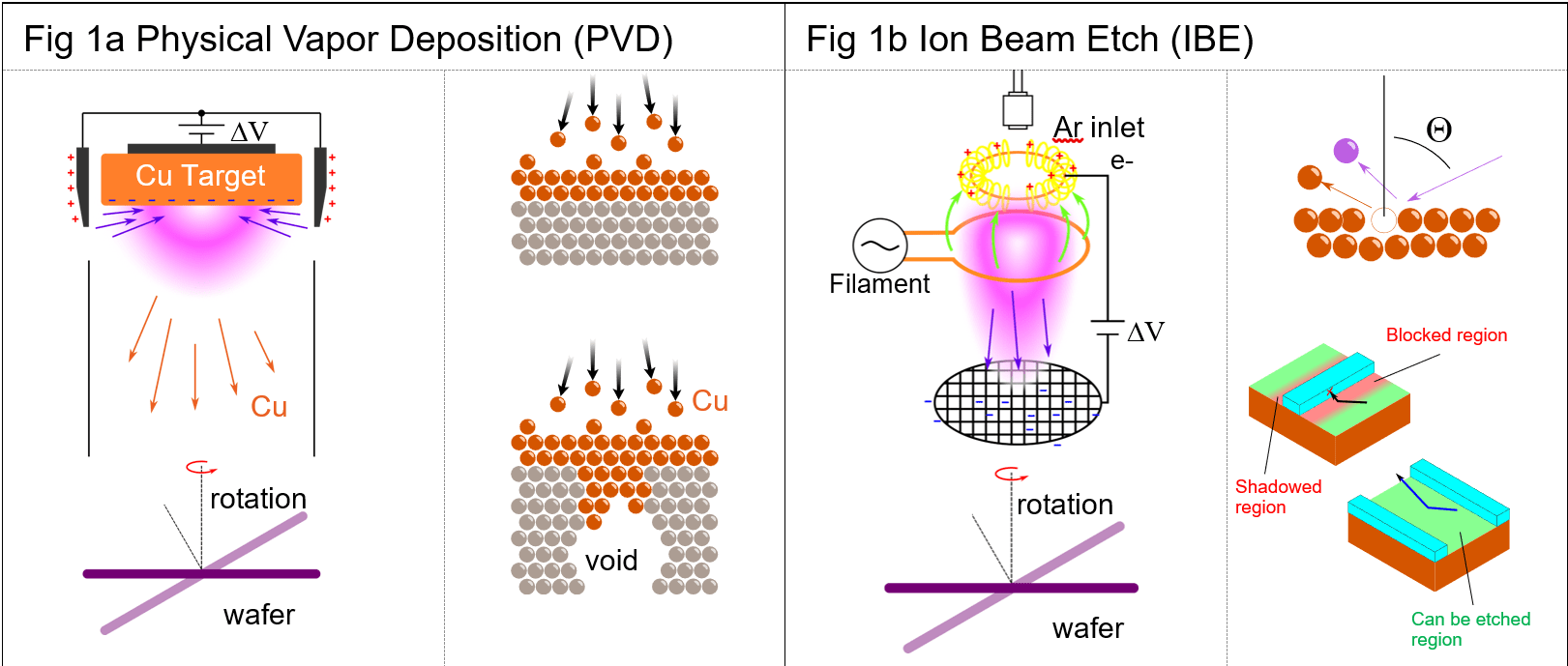
Fig. 1: (1a) Physical Vapor Deposition (PVD); (1b) Ion Beam Etch (IBE).
Process steps and virtual fabrication process
In order to understand the effect of deposition and etch on line resistance, we now model the PVD and IBE etch processes using SEMulator3D visibility deposition and etch functions. PVD was reproduced using a 30 degree angular spread visibility deposition process in SEMulator3D, which accurately models the random nature of ejected Cu atoms during bombardment with AR ions. IBE was reproduced in the model using a visibility etch with a 2 degree angular spread and a 60 degree polar angle tilt, to reflect the behavior of grid accelerated ions with low beam divergence. Both wafers are assumed to have free rotation. Other process steps have been adjusted in the virtual fabrication process to accommodate IBE and PVD constraints. Figure 2 displays the same structure created using both a damascene Cu fill (figure 2a) and PVD/IBE process (figure 2b). Additional process steps were included to incorporate certain limitations of PVD/IBE and create the equivalent shape for our desired end structures.


Fig. 2: (2a) Damascene fill Cu wire fabrication; (2b) PVD/IBE Cu wire fabrication.
We then demonstrate that an equivalent 16nm SRAM circuit cell can be fabricated with PVD/IBE wires while adhering to these limitations. Since all metal layers above the middle end of line are fabricated from a flat surface, this makes it an idea candidate for PVD/IBE wires, unlike the complex interconnect topologies seen in a finFET device. Figure 3 displays the isolated structure of each metal layer, and the necessary steps needed to create a three metal layer finFET structure using PVD/IBE.


Fig. 3: (3a) 16nm FinFET MEOL and 3 metal layers; (3b) Step by step metal layer fabrication via PVD/IBE.
Resistance results and conclusion
We then measure the electrical resistance of the wires from the topmost metal layer down to the vias of the finFET P and N channels, for both the damascene flow and physical vapor deposition. Figure 4 shows the starting point and ending point of the resistance measurement at the P and N channels (all other insulating materials are transparent). To compensate for the interface resistance between the TaN liner and the copper wire, the resistivity of copper was increased by using an exponential decay constant of 1 nm as a function of the nearest distance to the TaN interface. Since a damascene fill Cu deposition is not expected to be fully crystalline, the resistivity of Cu was increased by 50%. The PVD/IBE copper process does not use a TaN liner, so the exponential decay function was not applied, and the bulk resistivity of copper was used in this model. A table of resistivity comparing a Damascene flow vs. PVD is included in figure 4.

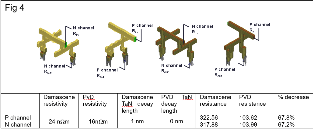
Fig. 4: Starting point and ending point of the resistance measurement at the P and N channels.
The resistance values calculated from our model state that we can achieve a 67% decrease in resistance using the IBE/PVD fabrication method compared to a conventional trench etch followed by damascene deposition. This occurs since no TaN liner is needed in IBE/PVD and there is lower CU resistivity during this process. Our results indicate that resistivity improvements can be achieved by using IBE/PVD compared to damascene fill during metal line formation, at the cost of a more complex fabrication process.

Timothy Yang
(सभी पद)
Timothy Yang is a software applications engineer at Coventor, a Lam Research Company. He works in process development, integration and yield improvement applications, with expertise in memory technologies. Prior to his work at Coventor, Yang worked at Tokyo Electron developing etch schemes, post lithography pattern improvement techniques, process flow control for SADP and SAQP patterning applications, and EUV and immersion lithography photoresist technology. Yang received his B.S. degree in physics from UCLA, an M.S. degree in Material Science from the Chiba Institute of Technology, and a Ph.D. degree in Material Science from Tohoku University.
- एसईओ संचालित सामग्री और पीआर वितरण। आज ही प्रवर्धित हो जाओ।
- प्लेटोब्लॉकचैन। Web3 मेटावर्स इंटेलिजेंस। ज्ञान प्रवर्धित। यहां पहुंचें।
- मिंटिंग द फ्यूचर डब्ल्यू एड्रिएन एशले। यहां पहुंचें।
- स्रोत: https://semiengineering.com/a-deposition-and-etch-technique-to-lower-resistance-of-semiconductor-metal-lines/
- :हैस
- :है
- ][पी
- 1
- 10
- 100
- a
- ऊपर
- त्वरित
- समायोजित
- सही रूप में
- पाना
- हासिल
- अतिरिक्त
- समायोजित
- सब
- सभी पद
- और
- कोणीय
- अनुप्रयोगों
- लागू
- AR
- हैं
- AS
- ग्रहण
- At
- परमाणु
- BE
- किरण
- हो जाता है
- किया गया
- के बीच
- सीमाओं
- by
- परिकलित
- कर सकते हैं
- उम्मीदवार
- नही सकता
- कुछ
- चैनलों
- कंपनी
- तुलना
- की तुलना
- जटिल
- स्थिर
- की कमी
- नियंत्रण
- परम्परागत
- तांबा
- लागत
- बनाना
- बनाया
- क्रिस्टल
- तिथि
- कमी
- गहरा
- डिग्री
- दिखाना
- निर्भर करता है
- पैसे जमा करने
- जमा किया
- वांछित
- विकासशील
- विकास
- युक्ति
- प्रसार
- प्रदर्शित करता है
- दूरी
- विचलन
- नीचे
- दौरान
- से प्रत्येक
- प्रभाव
- प्रभाव
- भी
- इंजीनियर
- बराबर
- EV
- अपेक्षित
- विशेषज्ञता
- घातीय
- विफलता
- आकृति
- भरना
- फ्लैट
- प्रवाह
- पीछा किया
- के लिए
- प्रपत्र
- निर्माण
- रूपों
- मुक्त
- से
- पूरी तरह से
- समारोह
- कार्यों
- ग्रिड
- है
- he
- हाई
- अत्यधिक
- छेद
- HTTPS
- विचार
- विसर्जन
- सुधार
- सुधार
- in
- घटना
- शामिल
- आवक
- सम्मिलित
- वृद्धि हुई
- बढ़ जाती है
- संकेत मिलता है
- संस्थान
- एकीकरण
- इंटरफेस
- पृथक
- IT
- आईटी इस
- जेपीजी
- पीटना
- परत
- परतों
- सीमाओं
- सीमित
- लाइन
- पंक्तियां
- लंबा
- निम्न
- बनाता है
- मुखौटा
- मास्क
- सामग्री
- सामग्री
- अधिकतम-चौड़ाई
- माप
- याद
- धातु
- तरीका
- मध्यम
- आदर्श
- मॉडल
- अधिक
- प्रकृति
- आवश्यक
- जरूरत
- of
- on
- आदेश
- अन्य
- हमारी
- समानांतर
- पथ
- पैटर्न
- भौतिक
- शारीरिक रूप से
- भौतिक विज्ञान
- प्लेटो
- प्लेटो डेटा इंटेलिजेंस
- प्लेटोडाटा
- बिन्दु
- ध्रुवीय
- पद
- पोस्ट
- को रोकने के
- पूर्व
- प्रक्रिया
- प्रक्रियाओं
- बिना सोचे समझे
- प्राप्त
- लाल
- प्रतिबिंबित
- क्षेत्रों
- हटाना
- अनुसंधान
- प्रतिरोध
- परिणाम
- s
- वही
- तराजू
- योजनाओं
- विज्ञान
- अर्धचालक
- आकार
- आकार
- आकार
- दिखाता है
- दृष्टि
- महत्वपूर्ण
- सिलिकॉन
- के बाद से
- एक
- छोटे
- So
- सॉफ्टवेयर
- विस्तार
- शुरुआत में
- राज्य
- कदम
- कदम
- संरचना
- इसके बाद
- सतह
- तालिका
- तकनीक
- टेक्नोलॉजीज
- टेक्नोलॉजी
- कि
- RSI
- इन
- तीन
- थंबनेल
- सेवा मेरे
- टोक्यो
- सर्वोच्च
- पारंपरिक रूप से
- पारदर्शी
- यूसीएलए
- समझना
- विश्वविद्यालय
- उपयोग
- प्रयुक्त
- उपयोग किया
- मान
- के माध्यम से
- वास्तविक
- दृश्यता
- परिवर्तनशील
- आयतन
- vs
- कौन कौन से
- जब
- मर्जी
- तार
- साथ में
- काम
- काम किया
- कार्य
- प्राप्ति
- जेफिरनेट