Le 24 janvier 2024
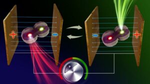
(Actualités Nanowerk) Researchers with the Department of Energy’s SLAC National Accelerator Laboratory, Stanford University and the DOE’s Lawrence Berkeley National Laboratory (LBNL) grew a twisted multilayer crystal structure for the first time and measured the structure’s key properties. The twisted structure could help researchers develop next-generation materials for solar cells, quantum computers, lasers and other devices.
“This structure is something that we have not seen before – it was a huge surprise to me,” said Yi Cui, a professor at Stanford and SLAC and paper co-author. “A new quantum electronic property could appear within this three-layer twisted structure in future experiments.”
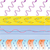
 LÉGENDE
Ajouter des calques, avec une touche d'originalité
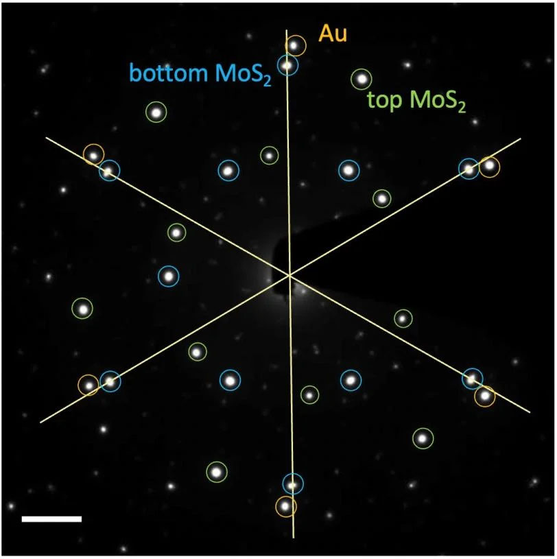
The crystals the team designed extended the concept of epitaxy, a phenomenon that occurs when one type of crystal material grows on top of another material in an ordered way – kind of like growing a neat lawn on top of soil, but at the atomic level. Understanding epitaxial growth has been critical to the development of many industries for more than 50 years, particularly the semiconductor industry. Indeed, epitaxy is part of many of the electronic devices that we use today, from cell phones to computers to solar panels, allowing electricity to flow, and not flow, through them. To date, epitaxy research has focused on growing one layer of material onto another, and the two materials have the same crystal orientation at the interface. This approach has been successful for decades in many applications, such as transistors, light-emitting diodes, lasers and quantum devices. But to find new materials that perform even better for more demanding needs, like quantum computing, researchers are searching for other epitaxial designs – ones that might be more complex, yet better performing, hence the “twisted epitaxy” concept demonstrated in this study. In their experiment, detailed in Sciences (“Twisted epitaxy of gold nanodisks grown between twisted substrate layers of molybdenum disulfide”), les chercheurs ont ajouté une couche d'or entre deux feuilles d'un matériau semi-conducteur traditionnel, le bisulfure de molybdène (MoS2). Because the top and bottom sheets were oriented differently, the gold atoms could not align with both simultaneously, which allowed the Au structure to twist, said Yi Cui, Professor Cui’s graduate student in materials science and engineering at Stanford and co-author of the paper. “With only a bottom MoS2 couche, l’or est heureux de s’aligner avec elle, donc aucune torsion ne se produit », a déclaré Cui, l’étudiant diplômé. "Mais avec deux MoS tordus2 feuilles, l'or n'est pas sûr de s'aligner avec la couche supérieure ou inférieure. Nous avons réussi à aider l'or à résoudre sa confusion et avons découvert une relation entre l'orientation de Au et l'angle de torsion du MoS bicouche.2. »Zapping des nanodisques d'or
Pour étudier la couche d'or en détail, l'équipe de chercheurs de l'Institut des sciences des matériaux et de l'énergie de Stanford (SIMES) et du LBNL a chauffé un échantillon de l'ensemble de la structure à 500 degrés Celsius. Ensuite, ils ont envoyé un flux d’électrons à travers l’échantillon à l’aide d’une technique appelée microscopie électronique à transmission (TEM), qui a révélé la morphologie, l’orientation et la déformation des nanodisques d’or après recuit à différentes températures. Mesurer ces propriétés des nanodisques d’or était une première étape nécessaire pour comprendre comment la nouvelle structure pourrait être conçue pour des applications réelles à l’avenir. "Sans cette étude, nous ne saurions pas s'il était possible de tordre une couche épitaxiale de métal sur un semi-conducteur", a déclaré Cui, l'étudiant diplômé. "La mesure de la structure complète à trois couches par microscopie électronique a confirmé que c'était non seulement possible, mais aussi que la nouvelle structure pouvait être contrôlée de manière passionnante." Ensuite, les chercheurs souhaitent étudier plus en profondeur les propriétés optiques des nanodisques d'or à l'aide de TEM et savoir si leur conception modifie les propriétés physiques telles que la structure des bandes de l'Au. Ils souhaitent également étendre ce concept pour tenter de construire des structures à trois couches avec d'autres matériaux semi-conducteurs et d'autres métaux. "Nous commençons à déterminer si seule cette combinaison de matériaux permet cela ou si cela se produit plus largement", a déclaré Bob Sinclair, professeur Charles M. Pigott à l'école de science et d'ingénierie des matériaux de Stanford et co-auteur de l'article. « Cette découverte ouvre une toute nouvelle série d’expériences que nous pouvons tenter. Nous pourrions être sur la bonne voie pour découvrir de toutes nouvelles propriétés matérielles que nous pourrions exploiter.- Contenu propulsé par le référencement et distribution de relations publiques. Soyez amplifié aujourd'hui.
- PlatoData.Network Ai générative verticale. Autonomisez-vous. Accéder ici.
- PlatoAiStream. Intelligence Web3. Connaissance Amplifiée. Accéder ici.
- PlatonESG. Carbone, Technologie propre, Énergie, Environnement, Solaire, La gestion des déchets. Accéder ici.
- PlatoHealth. Veille biotechnologique et essais cliniques. Accéder ici.
- La source: https://www.nanowerk.com/nanotechnology-news3/newsid=64500.php
- :possède
- :est
- :ne pas
- 10
- 13
- 14
- 24
- 50
- 50 ans
- 500
- 7
- 8
- 9
- a
- accélérateur
- ajouter
- ajoutée
- Après
- aligner
- permis
- Permettre
- permet
- aussi
- an
- ainsi que les
- Une autre
- apparaître
- applications
- une approche
- SONT
- AS
- At
- atomique
- BANDE
- BE
- car
- était
- before
- Début
- Berkeley
- Améliorée
- jusqu'à XNUMX fois
- grain
- tous les deux
- Bas et Leggings
- brand
- NOUVEAU
- largement
- construire
- mais
- appelé
- CAN
- cellule
- téléphones portables
- Cellules
- Celsius
- Canaux centraux
- Charles
- Coauteur
- combinaison
- complet
- complexe
- ordinateurs
- informatique
- concept
- CONFIRMÉ
- confusion
- contrôlée
- pourriez
- critique
- Cristal
- Date
- décennies
- exigeant
- démontré
- Département
- Conception
- un
- Avec nos Bagues Halo
- détail
- détaillé
- développer
- Développement
- Compatibles
- différent
- différemment
- découvert
- découverte
- DOE
- électricité
- Electronique
- électrons
- énergie
- ENGINEERING
- Pourtant, la
- passionnant
- expérience
- expériences
- Exploiter
- explorez
- étendre
- prolongé
- Trouvez
- trouver
- Prénom
- première fois
- flux
- concentré
- Pour
- de
- plus
- avenir
- Or
- diplôme
- a augmenté de
- Croissance
- cultivé
- Pousse
- Croissance
- arrive
- heureux vous
- Vous avez
- vous aider
- d'où
- Comment
- HTTPS
- majeur
- if
- image
- in
- secteurs
- industrie
- Institut
- Interfaces
- IT
- SES
- jpg
- ACTIVITES
- Genre
- Savoir
- laboratoire
- Luxinar SR AOM
- lawrence
- couche
- poules pondeuses
- APPRENTISSAGE
- Niveau
- comme
- gérés
- de nombreuses
- Matériel
- Conception matérielle
- matières premières.
- me
- mesuré
- mesure
- Métal
- Métaux
- Microscopie
- Milieu
- pourrait
- PLUS
- Nationales
- Soigné
- nécessaire
- Besoins
- Nouveauté
- next
- La prochaine génération
- aucune
- of
- on
- ONE
- et, finalement,
- uniquement
- ouverture
- or
- Autre
- nos
- panneaux
- Papier
- partie
- particulièrement
- effectuer
- effectuer
- phénomène
- téléphones
- Physique
- Platon
- Intelligence des données Platon
- PlatonDonnées
- possible
- Professeur
- propriétés
- propriété
- Quantum
- ordinateurs quantiques
- l'informatique quantique
- réal
- monde réel
- relation amoureuse
- un article
- chercheur
- chercheurs
- Révélé
- s
- Saïd
- même
- L'école
- Sciences
- STARFLEET SCIENCES
- recherche
- vu
- semi-conducteur
- envoyé
- Série
- feuilles
- simultanément
- So
- sol
- solaire
- Cellules solaires
- des panneaux solaires
- RÉSOUDRE
- quelque chose
- Stanford
- Stanford University
- étapes
- courant
- structure
- structures
- Étudiant
- Étude
- réussi
- tel
- sûr
- surprise
- équipe
- technique
- texte
- que
- qui
- Les
- El futuro
- leur
- Les
- puis
- Ces
- l'ont
- this
- Avec
- fiable
- à
- aujourd'hui
- top
- vers
- traditionnel
- Essai
- torsion
- deux
- type
- compréhension
- université
- utilisé
- en utilisant
- souhaitez
- était
- Façon..
- façons
- we
- ont été
- quand
- que
- qui
- la totalité
- comprenant
- dans les
- world
- pourra
- années
- encore
- zéphyrnet
Plus de Nanowerk
Les chercheurs ont développé une nouvelle méthode d’auto-assemblage pour fabriquer des nanofeuilles 2D multicouches
Nœud source: 3088801
Horodatage: Le 29 janvier 2024
Défauts de spin dans le nitrure de bore hexagonal créés par bombardement d'ions hélium
Nœud source: 2782123
Horodatage: Le 24 juillet 2023
Un «sandwich» particulier de graphène et de nitrure de bore pourrait conduire à la microélectronique de nouvelle génération
Nœud source: 2598354
Horodatage: 20 avril 2023
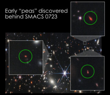
Le télescope spatial James Webb révèle des liens entre des galaxies proches et lointaines
Nœud source: 1889333
Horodatage: Le 9 janvier 2023
Lancer une nouvelle ère de nano-dispositifs accordables en couleur - la plus petite source de lumière jamais créée avec des couleurs commutables formées
Nœud source: 2801585
Horodatage: 3 août 2023
Améliorer l'évaluation de la sécurité des nanoparticules
Nœud source: 1867831
Horodatage: Le 4 janvier 2023
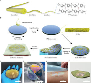
Une nouvelle « peau » ultra-fine pour l’électronique flexible promet des avancées pour les dispositifs médicaux et les prothèses
Nœud source: 3075264
Horodatage: Le 20 janvier 2024
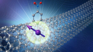
Le nanotube de carbone est idéal pour faire tourner des bits quantiques
Nœud source: 1995470
Horodatage: 6 Mar 2023
Le courant prend un chemin surprenant dans le matériau quantique
Nœud source: 2801583
Horodatage: 3 août 2023
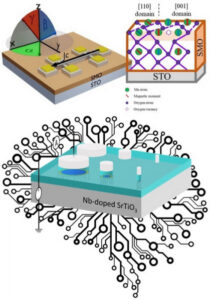
Les oxydes complexes pourraient alimenter les ordinateurs du futur
Nœud source: 1997462
Horodatage: 7 Mar 2023
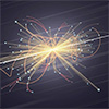
Un atome inhabituel aide à la recherche des éléments constitutifs de l'Univers
Nœud source: 1980749
Horodatage: 24 février 2023
La première antenne métasurface universelle au monde pour les communications 6G de haute sécurité
Nœud source: 3013617
Horodatage: Le 14 décembre 2023