17 年 2023 月 XNUMX 日 (Nanowerk新闻)我们生活在一个数据洪流的时代。用来存储和处理大量数据的数据中心需要消耗大量电力,这被称为环境污染的主要原因。为了克服这种情况,正在研究具有更低功耗和更高计算速度的多边形计算系统,但它们无法满足对数据处理的巨大需求,因为它们像传统的二进制计算系统一样以电信号进行操作。
研究人员开发了一种新型 2D-0D 半导体材料,可以充当由光脉冲供电的光学存储器。
该材料允许多种电阻状态,不像传统存储器那样只有 0 和 1 状态。
这可以实现系统的计算和存储部分之间的高速光学数据传输。
在测试中,光学存储器在 AI 模型上实现了 91% 的准确率,显示出了下一代计算的前景。
研究人员表示,这可能有助于克服硅半导体在人工智能和其他先进系统中的局限性。
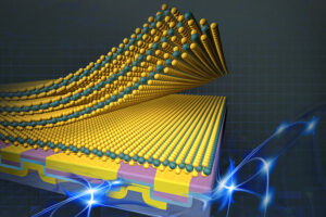
 2D-0D 混合光学存储设备。 (图片来源:KIST)
关键精华
2D-0D 混合光学存储设备。 (图片来源:KIST)
研究
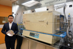
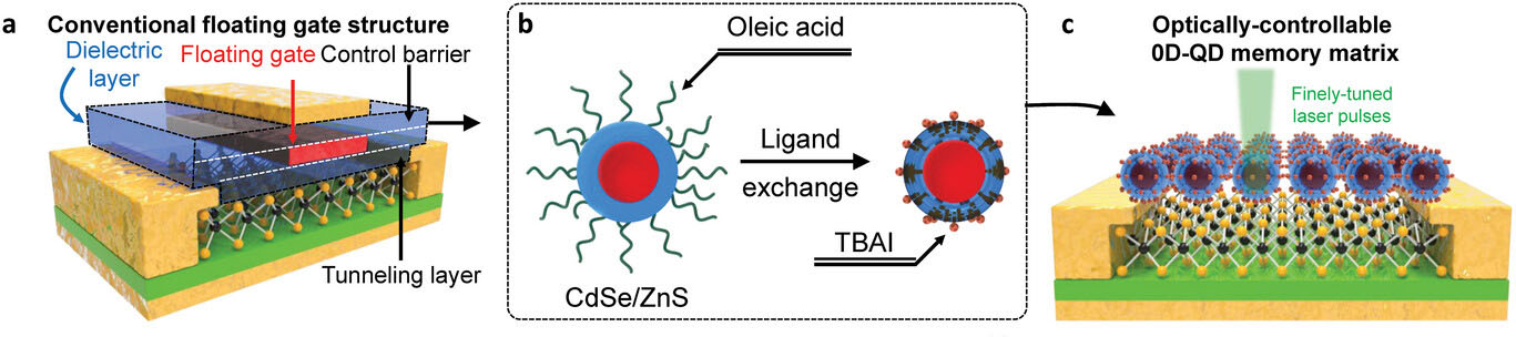
韩国科学技术研究院 (KIST) 宣布,大邱庆北科学技术学院光电材料与器件中心的 Do Kyung Hwang 博士和能源科学与工程系的 Jong-Soo Lee 教授( DGIST)联合开发了一种新型零维和二维(2D-0D)半导体人工结材料,并观察了光驱动的下一代存储器的效果。使用光而不是电信号在多层计算机的计算和存储部分之间传输数据可以显着提高处理速度。该研究发表于 先进材料 (“Probing optical multi-level memory effects in single core-shell quantum dots and application through 2D-0D hybrid inverters”)。研究团队通过加入 量子点 具有核壳结构,在硒化镉(CdSe)和硫化钼(MoS2)表面上有硫化锌(ZnS)2) semiconductor. The new material enables the storage and manipulation of electronic states within quantum dots measuring 10 nm or less. When light is applied to the cadmium selenide core, a certain number of electrons flow out of the molybdenum sulfide semiconductor, trapping holes in the core and making it conductive. The electron state inside cadmium selenide is also quantized. Intermittent light pulses trap electrons in the electron band one after the other, inducing a change in the resistance of the molybdenum sulfide through the field effect, and the resistance changes in a cascading manner depending on the number of light pulses. This process makes it possible to divide and maintain more than 0 and 10 states, unlike conventional memory, which has only 0 and 1 states. The zinc sulfide shell also prevents charge leakage between neighboring quantum dots, allowing each single quantum dot to function as a memory. While quantum dots in conventional 2D-0D semiconductor artificial junction structures simply amplify signals from light sensors, the team’s quantum dot structure perfectly mimics the floating gate memory structure, confirming its potential for use as a next-generation optical memory. The researchers verified the effectiveness of the polynomial memory phenomenon with neural network modeling using the CIFAR-10 dataset and achieved a 91% recognition rate. Dr. Hwang of KIST said, “The new multi-level optical memory device will contribute to accelerating the industrialization of next-generation system technologies such as artificial intelligence systems, which have been difficult to commercialize due to technical limitations arising from the miniaturization and integration of existing silicon semiconductor devices.”- :具有
- :是
- :不是
- 1
- 10
- 17
- 7
- 8
- 9
- a
- Able
- 加速
- 实现
- 高级
- 后
- AI
- 允许
- 允许
- 还
- 放大
- an
- 和
- 公布
- 应用领域
- 应用的
- 保健
- 人造的
- 人工智能
- AS
- At
- BAND
- 因为
- 很
- 作为
- 之间
- 但是
- by
- 被称为
- CAN
- Center
- 中心
- 一定
- 更改
- 更改
- 充
- 商业化
- 计算
- 一台
- 计算
- 消费
- 贡献
- 贡献者
- 常规
- 核心
- 可以
- data
- 数据中心
- 数据处理
- 日期
- 需求
- 问题类型
- 能源部
- 根据
- 发达
- 设备
- 设备
- 难
- 分
- do
- DOT
- dr
- 显着
- 两
- 每
- 效果
- 效用
- 影响
- 电力
- 电子
- 电子
- enable
- 使
- 使
- 能源
- 工程师
- 环境的
- 时代
- 醚(ETH)
- 现有
- 部分
- 漂浮的
- 洪水
- 流
- 针对
- 止
- 功能
- 处理
- 有
- 帮助
- 更高
- 孔
- HTTPS
- 巨大
- 杂交种
- 图片
- in
- 增加
- 内
- 研究所
- 积分
- 房源搜索
- IT
- 它的
- 加盟
- JPG
- 只是
- 韩国
- 李
- 减
- 光
- 喜欢
- 限制
- 生活
- 占地
- 降低
- 保持
- 主要
- 制作
- 制作
- 操作
- 方式
- 材料
- 物料
- 测量
- 回忆
- 内存
- 中间
- 模型
- 造型
- 更多
- 多
- 邻接
- 网络
- 神经
- 神经网络
- 全新
- 下一代
- 数
- 观察
- of
- on
- 一
- 仅由
- 操作
- 操作
- or
- 其他名称
- 输出
- 克服
- 部分
- 完美
- 现象
- PHP
- 柏拉图
- 柏拉图数据智能
- 柏拉图数据
- 污染
- 可能
- 潜力
- 功率
- 供电
- 防止
- 过程
- 处理
- 教授
- 承诺
- 出版
- 量子
- 量子点
- 量子点
- 率
- 宁
- 承认
- 研究
- 研究人员
- 抵制
- s
- 说
- 对工资盗窃
- 科学
- 科学与技术
- 半导体
- 半导体
- 传感器
- 壳
- 显示
- 信号
- 硅
- 只是
- 单
- 情况
- 速度
- 州/领地
- 州
- 存储
- 商店
- 结构体
- 结构
- 这样
- 磁化面
- 系统
- 产品
- 团队
- 文案
- 技术
- 专业技术
- 测试
- 比
- 这
- 他们
- Free Introduction
- 通过
- 至
- 诱捕
- 不像
- 使用
- 迎来
- 运用
- 专利
- we
- ,尤其是
- 这
- 而
- 将
- 中
- 和风网