17 ต.ค. 2023 (ข่าวนาโนเวิร์ค) เราอยู่ในยุคที่ข้อมูลล้นหลาม ศูนย์ข้อมูลที่ดำเนินการเพื่อจัดเก็บและประมวลผลข้อมูลจำนวนมากนี้ใช้พลังงานไฟฟ้าจำนวนมาก ซึ่งได้รับการขนานนามว่ามีส่วนสำคัญต่อมลภาวะต่อสิ่งแวดล้อม เพื่อเอาชนะสถานการณ์นี้ จึงได้มีการวิจัยระบบคอมพิวเตอร์หลายเหลี่ยมที่ใช้พลังงานน้อยลงและความเร็วในการคำนวณสูงขึ้น แต่ไม่สามารถรองรับความต้องการการประมวลผลข้อมูลจำนวนมากได้ เนื่องจากระบบทำงานด้วยสัญญาณไฟฟ้า เช่นเดียวกับระบบคอมพิวเตอร์ไบนารีทั่วไป
นักวิจัยได้พัฒนาวัสดุเซมิคอนดักเตอร์ 2D-0D ใหม่ที่สามารถทำหน้าที่เป็นหน่วยความจำแบบออปติคัลที่ขับเคลื่อนโดยพัลส์แสง
วัสดุนี้ช่วยให้มีสถานะต้านทานได้หลายสถานะ ทำให้มีสถานะมากกว่า 0 และ 1 เช่นเดียวกับหน่วยความจำทั่วไป
สิ่งนี้สามารถเปิดใช้งานการส่งข้อมูลออปติคัลความเร็วสูงระหว่างส่วนการประมวลผลและการจัดเก็บข้อมูลของระบบ
ในการทดสอบ หน่วยความจำแบบออปติคัลได้รับความแม่นยำ 91% ในโมเดล AI ซึ่งแสดงให้เห็นถึงแนวโน้มสำหรับการประมวลผลยุคต่อไป
นักวิจัยกล่าวว่าสิ่งนี้สามารถช่วยเอาชนะข้อจำกัดของเซมิคอนดักเตอร์ซิลิคอนสำหรับ AI และระบบขั้นสูงอื่นๆ
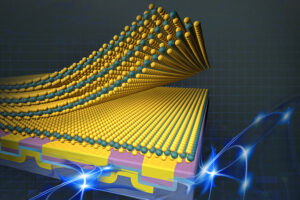
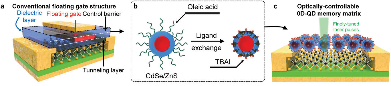 อุปกรณ์หน่วยความจำออปติคอลไฮบริด 2D-0D (ภาพ: KIST)
ประเด็นที่สำคัญ
อุปกรณ์หน่วยความจำออปติคอลไฮบริด 2D-0D (ภาพ: KIST)
วิจัย
สถาบันวิทยาศาสตร์และเทคโนโลยีแห่งเกาหลี (KIST) ประกาศว่า Dr. Do Kyung Hwang จากศูนย์วัสดุและอุปกรณ์ออปโตอิเล็กทรอนิกส์ และศาสตราจารย์ Jong-Soo Lee จากภาควิชาวิทยาศาสตร์พลังงานและวิศวกรรมศาสตร์ ที่สถาบันวิทยาศาสตร์และเทคโนโลยี Daegu Gyeongbuk ( DGIST) ได้ร่วมกันพัฒนาวัสดุแยกเทียมเซมิคอนดักเตอร์แบบศูนย์มิติและสองมิติ (2D-0D) ใหม่และสังเกตผลกระทบของหน่วยความจำยุคถัดไปที่ขับเคลื่อนด้วยแสง การส่งข้อมูลระหว่างส่วนคอมพิวเตอร์และส่วนจัดเก็บข้อมูลของคอมพิวเตอร์หลายระดับโดยใช้แสงแทนสัญญาณไฟฟ้าจะช่วยเพิ่มความเร็วในการประมวลผลได้อย่างมาก งานวิจัยที่ได้รับการตีพิมพ์ใน วัสดุขั้นสูง (“Probing optical multi-level memory effects in single core-shell quantum dots and application through 2D-0D hybrid inverters”). ทีมวิจัยได้ประดิษฐ์วัสดุแยกเทียมเซมิคอนดักเตอร์ 2D-0D ใหม่โดยการเข้าร่วม จุดควอนตัม ในโครงสร้างเปลือกแกนกลางที่มีซิงค์ซัลไฟด์ (ZnS) บนพื้นผิวของแคดเมียมซีลีไนด์ (CdSe) และโมลิบดีนัมซัลไฟด์ (MoS)2) semiconductor. The new material enables the storage and manipulation of electronic states within quantum dots measuring 10 nm or less. When light is applied to the cadmium selenide core, a certain number of electrons flow out of the molybdenum sulfide semiconductor, trapping holes in the core and making it conductive. The electron state inside cadmium selenide is also quantized. Intermittent light pulses trap electrons in the electron band one after the other, inducing a change in the resistance of the molybdenum sulfide through the field effect, and the resistance changes in a cascading manner depending on the number of light pulses. This process makes it possible to divide and maintain more than 0 and 10 states, unlike conventional memory, which has only 0 and 1 states. The zinc sulfide shell also prevents charge leakage between neighboring quantum dots, allowing each single quantum dot to function as a memory. While quantum dots in conventional 2D-0D semiconductor artificial junction structures simply amplify signals from light sensors, the team’s quantum dot structure perfectly mimics the floating gate memory structure, confirming its potential for use as a next-generation optical memory. The researchers verified the effectiveness of the polynomial memory phenomenon with neural network modeling using the CIFAR-10 dataset and achieved a 91% recognition rate. Dr. Hwang of KIST said, “The new multi-level optical memory device will contribute to accelerating the industrialization of next-generation system technologies such as artificial intelligence systems, which have been difficult to commercialize due to technical limitations arising from the miniaturization and integration of existing silicon semiconductor devices.”- เนื้อหาที่ขับเคลื่อนด้วย SEO และการเผยแพร่ประชาสัมพันธ์ รับการขยายวันนี้
- PlatoData.Network Vertical Generative Ai เพิ่มพลังให้กับตัวเอง เข้าถึงได้ที่นี่.
- เพลโตไอสตรีม. Web3 อัจฉริยะ ขยายความรู้ เข้าถึงได้ที่นี่.
- เพลโตESG. คาร์บอน, คลีนเทค, พลังงาน, สิ่งแวดล้อม แสงอาทิตย์, การจัดการของเสีย. เข้าถึงได้ที่นี่.
- เพลโตสุขภาพ เทคโนโลยีชีวภาพและข่าวกรองการทดลองทางคลินิก เข้าถึงได้ที่นี่.
- ที่มา: https://www.nanowerk.com/nanotechnology-news2/newsid=63861.php
- :มี
- :เป็น
- :ไม่
- 1
- 10
- 17
- 7
- 8
- 9
- a
- สามารถ
- เร่ง
- ความถูกต้อง
- ประสบความสำเร็จ
- สูง
- หลังจาก
- AI
- การอนุญาต
- ช่วยให้
- ด้วย
- ขยาย
- an
- และ
- ประกาศ
- การใช้งาน
- ประยุกต์
- เป็น
- เทียม
- ปัญญาประดิษฐ์
- AS
- At
- วงดนตรี
- เพราะ
- รับ
- กำลัง
- ระหว่าง
- แต่
- by
- ที่เรียกว่า
- CAN
- ศูนย์
- ศูนย์
- บาง
- เปลี่ยนแปลง
- การเปลี่ยนแปลง
- รับผิดชอบ
- ทำการค้า
- การคำนวณ
- คอมพิวเตอร์
- การคำนวณ
- การบริโภค
- สนับสนุน
- ผู้สนับสนุน
- ตามธรรมเนียม
- แกน
- ได้
- ข้อมูล
- ศูนย์ข้อมูล
- การประมวลผล
- วันที่
- ความต้องการ
- แผนก
- กระทรวงพลังงาน
- ทั้งนี้ขึ้นอยู่กับ
- พัฒนา
- เครื่อง
- อุปกรณ์
- ยาก
- แบ่ง
- do
- DOT
- dr
- เป็นคุ้งเป็นแคว
- สอง
- แต่ละ
- ผล
- ประสิทธิผล
- ผลกระทบ
- กระแสไฟฟ้า
- อิเล็กทรอนิกส์
- อิเล็กตรอน
- ทำให้สามารถ
- ช่วยให้
- การเปิดใช้งาน
- พลังงาน
- ชั้นเยี่ยม
- สิ่งแวดล้อม
- ยุค
- อีเธอร์ (ETH)
- ที่มีอยู่
- สนาม
- ที่ลอย
- น้ำท่วม
- ไหล
- สำหรับ
- ราคาเริ่มต้นที่
- ฟังก์ชัน
- จัดการ
- มี
- ช่วย
- สูงกว่า
- หลุม
- HTTPS
- ใหญ่
- เป็นลูกผสม
- ภาพ
- in
- เพิ่ม
- ภายใน
- สถาบัน
- บูรณาการ
- Intelligence
- IT
- ITS
- การร่วม
- jpg
- เพียงแค่
- เกาหลี
- Lee
- น้อยลง
- เบา
- กดไลก์
- ข้อ จำกัด
- สด
- Lot
- ลด
- เก็บรักษา
- สำคัญ
- ทำให้
- การทำ
- การจัดการ
- ลักษณะ
- วัสดุ
- วัสดุ
- การวัด
- ความทรงจำ
- หน่วยความจำ
- กลาง
- แบบ
- การสร้างแบบจำลอง
- ข้อมูลเพิ่มเติม
- หลาย
- ข้างเคียง
- เครือข่าย
- ประสาท
- เครือข่ายประสาท
- ใหม่
- รุ่นต่อไป
- จำนวน
- ตั้งข้อสังเกต
- of
- on
- ONE
- เพียง
- ทำงาน
- การดำเนินการ
- or
- อื่นๆ
- ออก
- เอาชนะ
- ส่วน
- อย่างสมบูรณ์
- ปรากฏการณ์
- PHP
- เพลโต
- เพลโตดาต้าอินเทลลิเจนซ์
- เพลโตดาต้า
- มลพิษ
- เป็นไปได้
- ที่มีศักยภาพ
- อำนาจ
- ขับเคลื่อน
- ป้องกัน
- กระบวนการ
- การประมวลผล
- ศาสตราจารย์
- คำมั่นสัญญา
- การตีพิมพ์
- ควอนตัม
- ควอนตัมดอท
- จุดควอนตัม
- คะแนน
- ค่อนข้าง
- การรับรู้
- การวิจัย
- นักวิจัย
- ความต้านทาน
- s
- กล่าวว่า
- กล่าว
- วิทยาศาสตร์
- วิทยาศาสตร์และเทคโนโลยี
- สารกึ่งตัวนำ
- อุปกรณ์กึ่งตัวนำ
- เซ็นเซอร์
- เปลือก
- การแสดง
- สัญญาณ
- ซิลิคอน
- ง่ายดาย
- เดียว
- สถานการณ์
- ความเร็ว
- สถานะ
- สหรัฐอเมริกา
- การเก็บรักษา
- จัดเก็บ
- โครงสร้าง
- โครงสร้าง
- อย่างเช่น
- พื้นผิว
- ระบบ
- ระบบ
- ทีม
- วิชาการ
- เทคโนโลยี
- เทคโนโลยี
- การทดสอบ
- กว่า
- ที่
- พื้นที่
- พวกเขา
- นี้
- ตลอด
- ไปยัง
- วางกับดัก
- แตกต่าง
- ใช้
- นำ
- การใช้
- การตรวจสอบแล้ว
- we
- เมื่อ
- ที่
- ในขณะที่
- จะ
- กับ
- ภายใน
- ลมทะเล
เพิ่มเติมจาก นาโนเวิร์ค
เปิดเผยขอบเขตระดับนาโน: สร้างสรรค์นวัตกรรมด้วยอิเล็กโทรดรุ่นนาโนรูพรุน
โหนดต้นทาง: 2700262
ประทับเวลา: มิถุนายน 2, 2023

เทคโนโลยีการเคลือบพื้นผิวใหม่ช่วยเพิ่มการปล่อยอิเล็กตรอนของวัสดุเจ็ดเท่า
โหนดต้นทาง: 2649550
ประทับเวลา: May 12, 2023


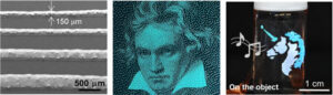
การแสดงการประสานเสียงแบบอินเทอร์แอกทีฟที่มีความละเอียดสูงที่ยืดหยุ่นได้สำหรับการเข้ารหัสด้วยภาพและเสียง
โหนดต้นทาง: 2931119
ประทับเวลา: ตุลาคม 12, 2023

ความแปลกประหลาดของกลศาสตร์ควอนตัม: อนาคตจะมีอิทธิพลต่ออดีตได้อย่างไร
โหนดต้นทาง: 1999524
ประทับเวลา: Mar 8, 2023
วิศวกร 'เติบโต' ทรานซิสเตอร์ที่บางระดับอะตอมบนชิปคอมพิวเตอร์
โหนดต้นทาง: 2612942
ประทับเวลา: เมษายน 27, 2023
หุ่นยนต์ 'ไร้สมอง' สามารถนำทางสิ่งกีดขวางที่ซับซ้อนได้ (พร้อมวิดีโอ)
โหนดต้นทาง: 2872212
ประทับเวลา: กันยายน 9, 2023
นักวิจัยรวมวัสดุ 2D ที่เปราะบางเข้ากับอุปกรณ์ได้อย่างปลอดภัย
โหนดต้นทาง: 3001717
ประทับเวลา: ธันวาคม 8, 2023
ไบโอเซนเซอร์เปลี่ยนวิธีการตรวจจับการปนเปื้อนของน้ำ
โหนดต้นทาง: 1946391
ประทับเวลา: กุมภาพันธ์ 8, 2023