หน้าแรก > ข่าวประชา > Novel design perovskite electrochemical cell for light-emission and light-detection
 |
| Dual-function Perovskite Silicon-integrated Electrochemical Cell CREDIT OAS |
นามธรรม:
A new publication from Opto-Electronic Advances, 10.29026/oea.2023.220154 discusses novel design perovskite electrochemical cell for light-emission and light-detection.
เซลล์ไฟฟ้าเคมี perovskite ออกแบบใหม่สำหรับการปล่อยแสงและการตรวจจับแสง
เสฉวน จีน | โพสต์เมื่อวันที่ 12 พฤษภาคม 2023
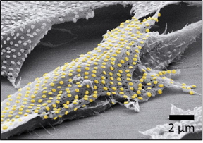
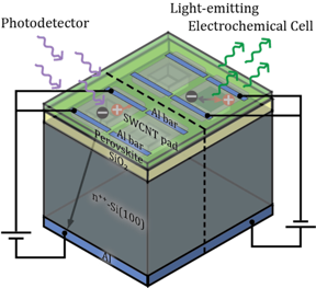
Although halide perovskite light-emitting devices exhibit exceptional properties such as high efficiency, high color purity, and broad color gamut, their industrial integration generally suffers from the technological complexity of devices’ multilayer structure alongside in-operation induced heating poor stability. Halide perovskite light-emitting electrochemical cells are a novel type of perovskite optoelectronic device that differs from the perovskite light-emitting diodes by a simple monolayered architecture. The reported in the paper perovskite light-emitting electrochemical cell consists of a silicon substrate, multifunctional single composite perovskite layer (a mixture of halide perovskite microcrystals, polymer support matrix, and added mobile ions), and transparent single-walled carbon nanotube film top contact. Due to silicon’s good thermal conductivity, the device endures 40% lower thermal heating during operation compared to conventional ITO/glass substrate. Moreover, when a positive bias is applied to the device it yields a luminance of more than 7000 cd/m2 at 523 nm (green color). When a negative bias is applied to the device it operates as a photodetector with a sensitivity up to 0.75 A/W (for wavelength in blue or UV regions), specific detectivity of 8.56∙1011 Jones, and linear dynamic range of 48 dB. The technological potential of such a device is proven by the demonstration of a 24-pixel indicator display as well as successful device miniaturization by the creation of electroluminescent images with the smallest features less than 50 μm.
The perovskite light-emitting electrochemical cells are a viable alternative to the conventional perovskite material devise research light-emitting diodes. Not only do perovskite light-emitting electrochemical cells imply having a much simpler architecture and design with one single functional layer replacing multiple active, charge-separation and transport layers of perovskite light-emitting diodes, but also perovskite light-emitting electrochemical cells can possess all extraordinary properties of LEDs, such as high efficiency, high color purity, and broad color gamut. The reason why perovskite light-emitting electrochemical cells are capable of doing that – is completely different from the LEDs operation principle: when electrical bias is applied to the device, mobile positive and negative ions inside of the perovskite layer migrate towards corresponding electrodes dynamically forming a p-i-n structure inside of the perovskite layer, which allows effective electron-hole recombination with photon emission! Comprehensive research on various back-ups to conventional LED technology is a valuable source of diversifying the pool of industrial opportunities.
The reported device demonstrates exceptional light-emitting and light-detecting (“dual-functionality”) characteristics alongside an enhanced in-operation heating durability. This is possible due to the utilization of silicon substrate in the perovskite light-emitting electrochemical cells design. Silicon material is one of the stepping stones of the CMOS technology – complementary metal–oxide–semiconductor technology – technology used in manufacturing of all semiconductor chips, displays, etc. Integration of such an emerging material like perovskite material with silicon brings the R&D community one step closer to obtaining an industrial perovskite light-emitting electrochemical cell.
Last but not least, the broader context benefit of the reported device design – is its ITO-free transparent electrode based on single-walled carbon nanotubes. ITO – Indium-Tin Oxide- is a transparent conductive material widely used in perovskite photovoltaics and optoelectronics. Indium is a depleting element and, thus, the replacement of ITO by other materials based on earth-abundant elements would aid to prevail the indium deficiency in the industry.
# # # # # # #
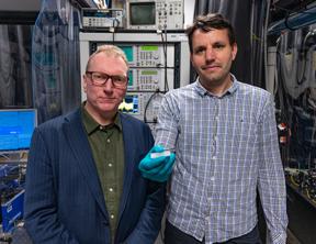
The project at hand results from a flourishing collaboration between Alferov University and ITMO University, both located in St.Petersburg (Russia). The purpose of the research group of Prof. Ivan Mukhin (Renewable Energy Sources Laboratory) from Alferov University is to extend the horizons of conventional semiconductors (Si and III-V group semiconductors) electronics and optoelectronics with innovative device designs (flexible and stretchable electronics) and with original ideas in material synthesis and manufacturing (taking advantage of low-dimensional structures such as semiconductor nanowires). The research group of Prof. Sergey Makarov (Laboratory of Hybrid Nanophotonics and Optoelectronics) from ITMO University not only focuses on fundamental research in the field of halide perovskite photonics and non-linear optics but also puts an enormous effort into the development of photovoltaic and optoelectronic perovskite devices, improvement of their stability and their industrial integration.
####
เกี่ยวกับบริษัท คอมพัสคริปท์ จำกัด
Opto-Electronic Advances (OEA) เป็นวารสาร SCI รายเดือนที่มีผลกระทบสูงและเข้าถึงได้แบบเปิด โดยมีปัจจัยผลกระทบที่ 8.933 (รายงานการอ้างอิงวารสารสำหรับ IF2021) นับตั้งแต่เปิดตัวในเดือนมีนาคม 2018 OEA ได้รับการจัดทำดัชนีในฐานข้อมูล SCI, EI, DOAJ, Scopus, CA และ ICI ตลอดเวลา และได้ขยายคณะกรรมการกองบรรณาธิการให้มีสมาชิก 36 รายจาก 17 ประเทศและภูมิภาค (ดัชนี h-index เฉลี่ย 49)
วารสารดังกล่าวจัดพิมพ์โดย The Institute of Optics and Electronics, Chinese Academy of Sciences โดยมีวัตถุประสงค์เพื่อเป็นเวทีสำหรับนักวิจัย นักวิชาการ ผู้เชี่ยวชาญ ผู้ปฏิบัติงาน และนักศึกษาในการให้ความรู้และแบ่งปันความรู้ในรูปแบบของเอกสารวิจัยเชิงประจักษ์และเชิงทฤษฎีคุณภาพสูงที่ครอบคลุม หัวข้อเกี่ยวกับทัศนศาสตร์ โฟโตนิกส์ และออปโตอิเล็กทรอนิกส์
สำหรับข้อมูลเพิ่มเติมกรุณาคลิก โปรดคลิกที่นี่เพื่ออ่านรายละเอียดเพิ่มเติม
ติดต่อ:
คอเนอร์ โลเวตต์
คอมพิวสคริปต์ บจก
สำนักงาน: 353-614 75205-
ลิขสิทธิ์ © Compuscript Ltd
หากคุณมีความคิดเห็นโปรด ติดต่อ เรา
ผู้ออกข่าวประชาสัมพันธ์ไม่ใช่ 7th Wave, Inc. หรือ Nanotechnology Now มีหน้าที่รับผิดชอบต่อความถูกต้องของเนื้อหา แต่เพียงผู้เดียว
บุ๊คมาร์ค:


| ลิงก์ที่เกี่ยวข้อง |
| ข่าวที่เกี่ยวข้อง |
ข่าวสารและข้อมูล
![]() การศึกษาแสดงให้เห็นว่า Ta2NiSe5 ไม่ใช่ฉนวน excitonic ทีมวิจัยระหว่างประเทศยุติการถกเถียงที่ยาวนานนับทศวรรษเกี่ยวกับต้นกำเนิดของสมมาตรที่แตกสลายในผลึกจำนวนมาก พฤษภาคม 12th, 2023
การศึกษาแสดงให้เห็นว่า Ta2NiSe5 ไม่ใช่ฉนวน excitonic ทีมวิจัยระหว่างประเทศยุติการถกเถียงที่ยาวนานนับทศวรรษเกี่ยวกับต้นกำเนิดของสมมาตรที่แตกสลายในผลึกจำนวนมาก พฤษภาคม 12th, 2023
![]() การเขียนโดยตรงด้วยเลเซอร์ของเซ็นเซอร์ความชื้นแบบยืดหยุ่นที่ใช้โลหะเหลว Ga2O3/GaXNUMXOXNUMX พฤษภาคม 12th, 2023
การเขียนโดยตรงด้วยเลเซอร์ของเซ็นเซอร์ความชื้นแบบยืดหยุ่นที่ใช้โลหะเหลว Ga2O3/GaXNUMXOXNUMX พฤษภาคม 12th, 2023
![]() ความก้าวหน้าในคุณสมบัติทางแสงของ MXenes – โครงสร้าง heterostructure สองมิติให้แนวคิดใหม่ พฤษภาคม 12th, 2023
ความก้าวหน้าในคุณสมบัติทางแสงของ MXenes – โครงสร้าง heterostructure สองมิติให้แนวคิดใหม่ พฤษภาคม 12th, 2023
เปรอฟสกี้
![]() เลเซอร์ perovskite กระจายความร้อนอย่างมีประสิทธิภาพโดยใช้ซับสเตรตเพชรที่มีค่าการนำความร้อนสูง เมษายน 14th, 2023
เลเซอร์ perovskite กระจายความร้อนอย่างมีประสิทธิภาพโดยใช้ซับสเตรตเพชรที่มีค่าการนำความร้อนสูง เมษายน 14th, 2023
![]() กลยุทธ์แบบผงต่อผงผู้ช่วย HCl สากลสำหรับการเตรียม perovskites ไร้สารตะกั่ว มีนาคม 24th, 2023
กลยุทธ์แบบผงต่อผงผู้ช่วย HCl สากลสำหรับการเตรียม perovskites ไร้สารตะกั่ว มีนาคม 24th, 2023
![]() ความเสถียรของเซลล์แสงอาทิตย์ perovskite มาถึงขั้นตอนถัดไป มกราคม 27th, 2023
ความเสถียรของเซลล์แสงอาทิตย์ perovskite มาถึงขั้นตอนถัดไป มกราคม 27th, 2023
![]() พอลิเมอร์ p-doping ปรับปรุงความเสถียรของเซลล์แสงอาทิตย์ perovskite มกราคม 20th, 2023
พอลิเมอร์ p-doping ปรับปรุงความเสถียรของเซลล์แสงอาทิตย์ perovskite มกราคม 20th, 2023
เทคโนโลยีการแสดงผล/ไฟ LED/ไฟ SS/OLED
![]() กลยุทธ์แบบผงต่อผงผู้ช่วย HCl สากลสำหรับการเตรียม perovskites ไร้สารตะกั่ว มีนาคม 24th, 2023
กลยุทธ์แบบผงต่อผงผู้ช่วย HCl สากลสำหรับการเตรียม perovskites ไร้สารตะกั่ว มีนาคม 24th, 2023
![]() ตัวถอดรหัสการพิมพ์ 3 มิติ การบีบอัดภาพที่เปิดใช้งาน AI สามารถเปิดใช้งานการแสดงผลที่มีความละเอียดสูงขึ้น ธันวาคม 9th, 2022
ตัวถอดรหัสการพิมพ์ 3 มิติ การบีบอัดภาพที่เปิดใช้งาน AI สามารถเปิดใช้งานการแสดงผลที่มีความละเอียดสูงขึ้น ธันวาคม 9th, 2022
อนาคตที่เป็นไปได้
![]() นักวิจัยที่ Purdue ค้นพบว่าภาพที่มีตัวนำยิ่งยวดนั้นแท้จริงแล้วเป็น 3 มิติและแฟร็กทัลที่ขับเคลื่อนด้วยความผิดปกติ พฤษภาคม 12th, 2023
นักวิจัยที่ Purdue ค้นพบว่าภาพที่มีตัวนำยิ่งยวดนั้นแท้จริงแล้วเป็น 3 มิติและแฟร็กทัลที่ขับเคลื่อนด้วยความผิดปกติ พฤษภาคม 12th, 2023
![]() การเขียนโดยตรงด้วยเลเซอร์ของเซ็นเซอร์ความชื้นแบบยืดหยุ่นที่ใช้โลหะเหลว Ga2O3/GaXNUMXOXNUMX พฤษภาคม 12th, 2023
การเขียนโดยตรงด้วยเลเซอร์ของเซ็นเซอร์ความชื้นแบบยืดหยุ่นที่ใช้โลหะเหลว Ga2O3/GaXNUMXOXNUMX พฤษภาคม 12th, 2023
![]() ความก้าวหน้าในคุณสมบัติทางแสงของ MXenes – โครงสร้าง heterostructure สองมิติให้แนวคิดใหม่ พฤษภาคม 12th, 2023
ความก้าวหน้าในคุณสมบัติทางแสงของ MXenes – โครงสร้าง heterostructure สองมิติให้แนวคิดใหม่ พฤษภาคม 12th, 2023
การค้นพบ
![]() การศึกษาแสดงให้เห็นว่า Ta2NiSe5 ไม่ใช่ฉนวน excitonic ทีมวิจัยระหว่างประเทศยุติการถกเถียงที่ยาวนานนับทศวรรษเกี่ยวกับต้นกำเนิดของสมมาตรที่แตกสลายในผลึกจำนวนมาก พฤษภาคม 12th, 2023
การศึกษาแสดงให้เห็นว่า Ta2NiSe5 ไม่ใช่ฉนวน excitonic ทีมวิจัยระหว่างประเทศยุติการถกเถียงที่ยาวนานนับทศวรรษเกี่ยวกับต้นกำเนิดของสมมาตรที่แตกสลายในผลึกจำนวนมาก พฤษภาคม 12th, 2023
![]() การเขียนโดยตรงด้วยเลเซอร์ของเซ็นเซอร์ความชื้นแบบยืดหยุ่นที่ใช้โลหะเหลว Ga2O3/GaXNUMXOXNUMX พฤษภาคม 12th, 2023
การเขียนโดยตรงด้วยเลเซอร์ของเซ็นเซอร์ความชื้นแบบยืดหยุ่นที่ใช้โลหะเหลว Ga2O3/GaXNUMXOXNUMX พฤษภาคม 12th, 2023
![]() ความก้าวหน้าในคุณสมบัติทางแสงของ MXenes – โครงสร้าง heterostructure สองมิติให้แนวคิดใหม่ พฤษภาคม 12th, 2023
ความก้าวหน้าในคุณสมบัติทางแสงของ MXenes – โครงสร้าง heterostructure สองมิติให้แนวคิดใหม่ พฤษภาคม 12th, 2023
ประกาศ
![]() การศึกษาแสดงให้เห็นว่า Ta2NiSe5 ไม่ใช่ฉนวน excitonic ทีมวิจัยระหว่างประเทศยุติการถกเถียงที่ยาวนานนับทศวรรษเกี่ยวกับต้นกำเนิดของสมมาตรที่แตกสลายในผลึกจำนวนมาก พฤษภาคม 12th, 2023
การศึกษาแสดงให้เห็นว่า Ta2NiSe5 ไม่ใช่ฉนวน excitonic ทีมวิจัยระหว่างประเทศยุติการถกเถียงที่ยาวนานนับทศวรรษเกี่ยวกับต้นกำเนิดของสมมาตรที่แตกสลายในผลึกจำนวนมาก พฤษภาคม 12th, 2023
![]() การเขียนโดยตรงด้วยเลเซอร์ของเซ็นเซอร์ความชื้นแบบยืดหยุ่นที่ใช้โลหะเหลว Ga2O3/GaXNUMXOXNUMX พฤษภาคม 12th, 2023
การเขียนโดยตรงด้วยเลเซอร์ของเซ็นเซอร์ความชื้นแบบยืดหยุ่นที่ใช้โลหะเหลว Ga2O3/GaXNUMXOXNUMX พฤษภาคม 12th, 2023
![]() ความก้าวหน้าในคุณสมบัติทางแสงของ MXenes – โครงสร้าง heterostructure สองมิติให้แนวคิดใหม่ พฤษภาคม 12th, 2023
ความก้าวหน้าในคุณสมบัติทางแสงของ MXenes – โครงสร้าง heterostructure สองมิติให้แนวคิดใหม่ พฤษภาคม 12th, 2023
บทสัมภาษณ์ / บทวิจารณ์หนังสือ / บทความ / รายงาน / พ็อดคาสท์ / วารสาร / เอกสารปกขาว / โปสเตอร์
![]() นักวิจัยที่ Purdue ค้นพบว่าภาพที่มีตัวนำยิ่งยวดนั้นแท้จริงแล้วเป็น 3 มิติและแฟร็กทัลที่ขับเคลื่อนด้วยความผิดปกติ พฤษภาคม 12th, 2023
นักวิจัยที่ Purdue ค้นพบว่าภาพที่มีตัวนำยิ่งยวดนั้นแท้จริงแล้วเป็น 3 มิติและแฟร็กทัลที่ขับเคลื่อนด้วยความผิดปกติ พฤษภาคม 12th, 2023
![]() การเขียนโดยตรงด้วยเลเซอร์ของเซ็นเซอร์ความชื้นแบบยืดหยุ่นที่ใช้โลหะเหลว Ga2O3/GaXNUMXOXNUMX พฤษภาคม 12th, 2023
การเขียนโดยตรงด้วยเลเซอร์ของเซ็นเซอร์ความชื้นแบบยืดหยุ่นที่ใช้โลหะเหลว Ga2O3/GaXNUMXOXNUMX พฤษภาคม 12th, 2023
![]() ความก้าวหน้าในคุณสมบัติทางแสงของ MXenes – โครงสร้าง heterostructure สองมิติให้แนวคิดใหม่ พฤษภาคม 12th, 2023
ความก้าวหน้าในคุณสมบัติทางแสงของ MXenes – โครงสร้าง heterostructure สองมิติให้แนวคิดใหม่ พฤษภาคม 12th, 2023
- เนื้อหาที่ขับเคลื่อนด้วย SEO และการเผยแพร่ประชาสัมพันธ์ รับการขยายวันนี้
- เพลโตไอสตรีม. ข้อมูลอัจฉริยะ Web3 ขยายความรู้ เข้าถึงได้ที่นี่.
- การสร้างอนาคตโดย Adryenn Ashley เข้าถึงได้ที่นี่.
- ซื้อและขายหุ้นในบริษัท PRE-IPO ด้วย PREIPO® เข้าถึงได้ที่นี่.
- ที่มา: http://www.nanotech-now.com/news.cgi?story_id=57337
- :มี
- :เป็น
- :ไม่
- $ ขึ้น
- 10
- 2018
- 2023
- 26
- 27th
- 2D
- วัสดุ 2 มิติ
- 3d
- 49
- 50
- 8
- 9th
- a
- วิทยาลัย
- เข้า
- ความถูกต้อง
- ข้าม
- คล่องแคล่ว
- จริง
- ที่เพิ่ม
- ความก้าวหน้า
- ความได้เปรียบ
- ช่วย
- การเล็ง
- ทั้งหมด
- ช่วยให้
- คู่ขนาน
- ด้วย
- ทางเลือก
- an
- และ
- ประกาศ
- ประยุกต์
- เมษายน
- สถาปัตยกรรม
- เป็น
- รอบ
- AS
- At
- เฉลี่ย
- ตาม
- รับ
- ประโยชน์
- ระหว่าง
- อคติ
- สีน้ำเงิน
- คณะกรรมการ
- ทั้งสอง
- หมดสภาพ
- นำ
- กว้าง
- ที่กว้างขึ้น
- มหาวิทยาลัยบราวน์
- แต่
- by
- CA
- CAN
- สามารถ
- คาร์บอน
- ท่อนาโนคาร์บอน
- เซลล์
- ศูนย์
- CGI
- ลักษณะ
- สาธารณรัฐประชาชนจีน
- ชาวจีน
- ชิป
- คลิก
- ใกล้ชิด
- การทำงานร่วมกัน
- สี
- COM
- ความเห็น
- ชุมชน
- เมื่อเทียบกับ
- ประกอบ
- อย่างสมบูรณ์
- ความซับซ้อน
- ครอบคลุม
- การนำ
- ติดต่อเรา
- เนื้อหา
- สิ่งแวดล้อม
- ตามธรรมเนียม
- ตรงกัน
- ได้
- ประเทศ
- ครอบคลุม
- การสร้าง
- เครดิต
- ฐานข้อมูล
- การอภิปราย
- ธันวาคม
- แสดงให้เห็นถึง
- ออกแบบ
- การออกแบบ
- พัฒนาการ
- เครื่อง
- อุปกรณ์
- เงินตรา
- เพชร
- ต่าง
- โดยตรง
- ค้นพบ
- แสดง
- แสดง
- do
- การทำ
- สอง
- ความทนทาน
- ในระหว่าง
- พลวัต
- แบบไดนามิก
- บทบรรณาธิการ
- มีประสิทธิภาพ
- อย่างมีประสิทธิภาพ
- ความพยายาม
- อิเล็กทรอนิกส์
- ธาตุ
- องค์ประกอบ
- กากกะรุน
- ทำให้สามารถ
- ปลาย
- พลังงาน
- ที่เพิ่มขึ้น
- มหาศาล
- ฯลฯ
- อีเธอร์ (ETH)
- เป็นพิเศษ
- แสดง
- ขยาย
- ขยายออก
- พิเศษ
- ปัจจัย
- คุณสมบัติ
- สนาม
- ฟิล์ม
- ชื่อจริง
- ครั้งแรก
- มีความยืดหยุ่น
- มุ่งเน้นไปที่
- สำหรับ
- ฟอร์ม
- พบ
- ราคาเริ่มต้นที่
- การทำงาน
- พื้นฐาน
- โดยทั่วไป
- GIF
- ทองคำ
- ดี
- แกรฟีน
- สีเขียว
- บัญชีกลุ่ม
- มือ
- มี
- มี
- จุดสูง
- ไกลโพ้น
- ที่ http
- HTTPS
- เป็นลูกผสม
- ความคิด
- if
- ภาพ
- ภาพ
- ส่งผลกระทบ
- การปรับปรุง
- ช่วยเพิ่ม
- in
- อิงค์
- ตัวบ่งชี้
- อุตสาหกรรม
- อุตสาหกรรม
- ข้อมูล
- นวัตกรรม
- สถาบัน
- บูรณาการ
- International
- เข้าไป
- IT
- ITS
- มกราคม
- วารสาร
- ความรู้
- ห้องปฏิบัติการ
- เลเซอร์
- เปิดตัว
- ชั้น
- ชั้น
- น้อยที่สุด
- นำ
- น้อยลง
- กดไลก์
- การเชื่อมโยง
- ที่ตั้งอยู่
- ยาวนาน
- การผลิต
- หลาย
- มีนาคม
- วัสดุ
- วัสดุ
- มดลูก
- อาจ..
- สมาชิก
- วิธี
- อพยพ
- สารผสม
- โทรศัพท์มือถือ
- รายเดือน
- ข้อมูลเพิ่มเติม
- ยิ่งไปกว่านั้น
- มาก
- หลาย
- nanophotonics
- นาโนเทคโนโลยี
- เชิงลบ
- สุทธิ
- ใหม่
- ข่าว
- ถัดไป
- นวนิยาย
- ตอนนี้
- การได้รับ
- of
- on
- ONE
- เพียง
- เปิด
- ดำเนินการ
- การดำเนินการ
- โอกาส
- เลนส์
- or
- ที่มา
- เป็นต้นฉบับ
- อื่นๆ
- เกิน
- กระดาษ
- เอกสาร
- ลูกแพร์
- ปีเตอร์เบิร์ก
- PHP
- เวที
- เพลโต
- เพลโตดาต้าอินเทลลิเจนซ์
- เพลโตดาต้า
- กรุณา
- พอลิเมอ
- สระ
- น่าสงสาร
- บวก
- เป็นไปได้
- โพสต์
- โพสต์
- ที่มีศักยภาพ
- การเตรียมความพร้อม
- กด
- ข่าวประชาสัมพันธ์
- หลัก
- การสอบสวน
- มืออาชีพ
- โครงการ
- คุณสมบัติ
- ที่พิสูจน์แล้ว
- ให้
- การให้
- สิ่งพิมพ์
- การตีพิมพ์
- การประกาศ
- วัตถุประสงค์
- ทำให้
- คุณภาพ
- ควอนตัม
- ข้อมูลควอนตัม
- วิจัยและพัฒนา
- พิสัย
- อย่างรวดเร็ว
- ต้นน้ำ
- เหตุผล
- ภูมิภาค
- ปล่อย
- สัมพันธ์
- ทดแทน
- พลังงานทดแทน
- การแทนที่
- รายงาน
- รายงาน
- การวิจัย
- กลุ่มวิจัย
- นักวิจัย
- รับผิดชอบ
- ผลสอบ
- กลับ
- สุดท้าย
- รัสเซีย
- s
- ลด
- SCI
- วิทยาศาสตร์
- วิทยาศาสตร์
- นักวิทยาศาสตร์
- ค้นหา
- ภาค
- สารกึ่งตัวนำ
- อุปกรณ์กึ่งตัวนำ
- ความไว
- ตกตะกอน
- Share
- เสฉวน
- ซิลิคอน
- ง่าย
- ตั้งแต่
- เดียว
- โซลา
- พลังงานแสงอาทิตย์
- แหล่ง
- แหล่งที่มา
- โดยเฉพาะ
- สปิน
- Stability
- เริ่มต้น
- ขั้นตอน
- ก้าว
- หิน
- กลยุทธ์
- โครงสร้าง
- นักเรียน
- ส่ง
- ที่ประสบความสำเร็จ
- อย่างเช่น
- ทนทุกข์ทรมาน
- สนับสนุน
- การ
- ทีม
- เทคโนโลยี
- เทคโนโลยี
- กว่า
- ที่
- พื้นที่
- ของพวกเขา
- ตามทฤษฎี
- ร้อน
- นี้
- เวลา
- ไปยัง
- ด้านบน
- หัวข้อ
- ไปทาง
- โปร่งใส
- การขนส่ง
- ชนิด
- สากล
- มหาวิทยาลัย
- us
- มือสอง
- การใช้
- มีคุณค่า
- ต่างๆ
- ทำงานได้
- คลื่น
- ดี
- เมื่อ
- ที่
- ทำไม
- อย่างกว้างขวาง
- กับ
- จะ
- การเขียน
- yahoo
- อัตราผลตอบแทน
- เธอ
- ลมทะเล