ข่าว: อิเล็กทรอนิคขนาดเล็ก
24 พฤษภาคม 2023
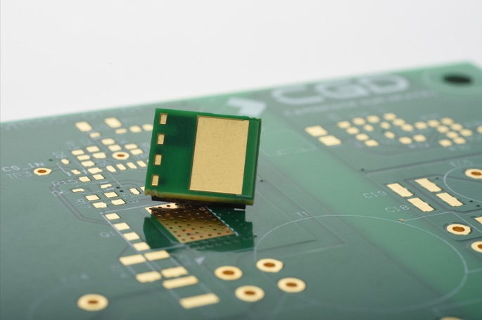
Cambridge GaN Devices Ltd (CGD) — which was spun out of the University of Cambridge Department of Engineering’s Electrical Power and Energy Conversion group in 2016 and designs, develops and commercializes power transistors and ICs that use GaN-on-silicon substrates — has introduced a range of Application Interface Boards that allow designers to try out its ICeGaN high-electron-mobility transistors (HEMTs) in existing circuits in place of competing MOSFET or GaN devices without having to re-layout the PCB.
Application Interface Boards are adaptor PCBs that are soldered to an ICeGaN device, which map each pin/signal from the ICeGaN HEMT footprint to the corresponding pins/signals of an alternative component footprint.
“These Application Interface Boards are designed for design and evaluation purposes only, of course. This is a quick, first step to enable the user to put one of our ICeGaN ICs into an existing design,” says Peter Comiskey, director of application engineering. “There is some minor impact on thermal performance, but surprisingly little difference in EMC or electrical performance.”
CGD offers Application Interface Boards for a number of industry-standard devices from leading MOSFET and GaN device makers. A full list can be found on the คู่มือผู้ใช้, but the firm can also develop an Application Interface Board for devices not currently supported for delivery within four weeks.
ICeGaN HEMT ของ CGD มีปริมาณมาก
- เนื้อหาที่ขับเคลื่อนด้วย SEO และการเผยแพร่ประชาสัมพันธ์ รับการขยายวันนี้
- เพลโตไอสตรีม. ข้อมูลอัจฉริยะ Web3 ขยายความรู้ เข้าถึงได้ที่นี่.
- การสร้างอนาคตโดย Adryenn Ashley เข้าถึงได้ที่นี่.
- ซื้อและขายหุ้นในบริษัท PRE-IPO ด้วย PREIPO® เข้าถึงได้ที่นี่.
- ที่มา: https://www.semiconductor-today.com/news_items/2023/may/cgd-240523.shtml
- :มี
- :เป็น
- :ไม่
- 2016
- a
- อนุญาต
- ด้วย
- ทางเลือก
- an
- และ
- การใช้งาน
- เป็น
- ใช้ได้
- BE
- คณะกรรมการ
- แต่
- เคมบริดจ์
- CAN
- การแข่งขัน
- ส่วนประกอบ
- การแปลง
- ตรงกัน
- หลักสูตร
- ขณะนี้
- การจัดส่ง
- แผนก
- ออกแบบ
- ได้รับการออกแบบ
- นักออกแบบ
- การออกแบบ
- พัฒนา
- พัฒนา
- เครื่อง
- อุปกรณ์
- ความแตกต่าง
- ผู้อำนวยการ
- แต่ละ
- ทำให้สามารถ
- พลังงาน
- ชั้นเยี่ยม
- การประเมินผล
- ที่มีอยู่
- บริษัท
- ชื่อจริง
- รอยพระบาท
- สำหรับ
- พบ
- สี่
- ราคาเริ่มต้นที่
- เต็ม
- บัญชีกลุ่ม
- มี
- จุดสูง
- ที่ http
- HTTPS
- ICS
- ส่งผลกระทบ
- in
- อินเตอร์เฟซ
- เข้าไป
- แนะนำ
- เปิดตัว
- รายการ
- ITS
- jpg
- ชั้นนำ
- รายการ
- น้อย
- จำกัด
- ผู้ผลิต
- แผนที่
- อาจ..
- ผู้เยาว์
- จำนวน
- of
- เสนอ
- on
- ONE
- เพียง
- or
- ของเรา
- ออก
- ซีบีเอส
- รูปแบบไฟล์ PDF
- การปฏิบัติ
- พีเตอร์
- สถานที่
- เพลโต
- เพลโตดาต้าอินเทลลิเจนซ์
- เพลโตดาต้า
- อำนาจ
- วัตถุประสงค์
- ใส่
- รวดเร็ว
- พิสัย
- ที่เกี่ยวข้อง
- พูดว่า
- บาง
- ปั่น
- ขั้นตอน
- ที่สนับสนุน
- ที่
- พื้นที่
- ร้อน
- นี้
- ไปยัง
- ลอง
- มหาวิทยาลัย
- มหาวิทยาลัยเคมบริดจ์
- ใช้
- ผู้ใช้งาน
- คือ
- สัปดาห์ที่ผ่านมา
- ที่
- ภายใน
- ไม่มี
- ลมทะเล