Jan 24, 2024
(Nanowerk novice) Researchers with the Department of Energy’s SLAC National Accelerator Laboratory, Stanford University and the DOE’s Lawrence Berkeley National Laboratory (LBNL) grew a twisted multilayer crystal structure for the first time and measured the structure’s key properties. The twisted structure could help researchers develop next-generation materials for solar cells, quantum computers, lasers and other devices.
“This structure is something that we have not seen before – it was a huge surprise to me,” said Yi Cui, a professor at Stanford and SLAC and paper co-author. “A new quantum electronic property could appear within this three-layer twisted structure in future experiments.”
 NAPIS
NAPIS
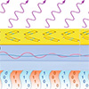
Dodajanje plasti, s preobratom
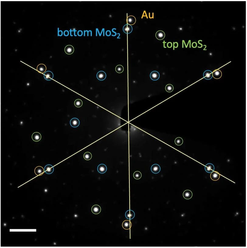
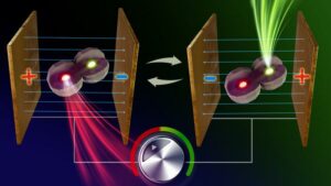
The crystals the team designed extended the concept of epitaxy, a phenomenon that occurs when one type of crystal material grows on top of another material in an ordered way – kind of like growing a neat lawn on top of soil, but at the atomic level. Understanding epitaxial growth has been critical to the development of many industries for more than 50 years, particularly the semiconductor industry. Indeed, epitaxy is part of many of the electronic devices that we use today, from cell phones to computers to solar panels, allowing electricity to flow, and not flow, through them. To date, epitaxy research has focused on growing one layer of material onto another, and the two materials have the same crystal orientation at the interface. This approach has been successful for decades in many applications, such as transistors, light-emitting diodes, lasers and quantum devices. But to find new materials that perform even better for more demanding needs, like quantum computing, researchers are searching for other epitaxial designs – ones that might be more complex, yet better performing, hence the “twisted epitaxy” concept demonstrated in this study. In their experiment, detailed in Znanost (“Twisted epitaxy of gold nanodisks grown between twisted substrate layers of molybdenum disulfide”), so raziskovalci dodali plast zlata med dve plošči tradicionalnega polprevodniškega materiala, molibdenovega disulfida (MoS2). Because the top and bottom sheets were oriented differently, the gold atoms could not align with both simultaneously, which allowed the Au structure to twist, said Yi Cui, Professor Cui’s graduate student in materials science and engineering at Stanford and co-author of the paper. “With only a bottom MoS2 plasti, se zlato z veseljem poravna z njo, tako da ne pride do zasuka,« je dejal Cui, podiplomski študent. »Ampak z dvema zvitima MoS2 listov, zlato ni gotovo poravnano z zgornjo ali spodnjo plastjo. Zlatu smo uspeli pomagati rešiti njegovo zmedo in odkrili smo razmerje med orientacijo Au in zasučnim kotom dvoslojnega MoS2«.Zapiranje zlatih nanodiskov
Da bi podrobno preučili zlato plast, je skupina raziskovalcev s Stanfordskega inštituta za materiale in energetske znanosti (SIMES) in LBNL segrela vzorec celotne strukture na 500 stopinj Celzija. Nato so poslali tok elektronov skozi vzorec s tehniko, imenovano transmisijska elektronska mikroskopija (TEM), ki je razkrila morfologijo, orientacijo in napetost zlatih nanodiskov po žarjenju pri različnih temperaturah. Merjenje teh lastnosti zlatih nanodiskov je bil nujen prvi korak k razumevanju, kako bi lahko novo strukturo oblikovali za aplikacije v resničnem svetu v prihodnosti. "Brez te študije ne bi vedeli, ali je zvijanje epitaksialne plasti kovine na vrhu polprevodnika sploh mogoče," je dejal Cui, podiplomski študent. "Merjenje celotne trislojne strukture z elektronsko mikroskopijo je potrdilo, da ni le mogoče, ampak tudi, da je mogoče novo strukturo nadzorovati na razburljive načine." Nato želijo raziskovalci nadalje preučiti optične lastnosti zlatih nanodiskov z uporabo TEM in izvedeti, ali njihova zasnova spreminja fizične lastnosti, kot je pasovna struktura Au. Prav tako želijo razširiti ta koncept, da bi poskušali zgraditi trislojne strukture z drugimi polprevodniškimi materiali in drugimi kovinami. "Začenjamo raziskovati, ali to omogoča le ta kombinacija materialov ali pa se to zgodi širše," je dejal Bob Sinclair, profesor Charlesa M. Pigotta na Stanfordovi šoli za znanost in inženirstvo materialov in soavtor prispevka. »To odkritje odpira povsem novo serijo poskusov, ki jih lahko poskusimo. Lahko bi bili na poti k iskanju popolnoma novih lastnosti materiala, ki bi jih lahko izkoristili.«- Distribucija vsebine in PR s pomočjo SEO. Okrepite se še danes.
- PlatoData.Network Vertical Generative Ai. Opolnomočite se. Dostopite tukaj.
- PlatoAiStream. Web3 Intelligence. Razširjeno znanje. Dostopite tukaj.
- PlatoESG. Ogljik, CleanTech, Energija, Okolje, sončna energija, Ravnanje z odpadki. Dostopite tukaj.
- PlatoHealth. Obveščanje o biotehnologiji in kliničnih preskušanjih. Dostopite tukaj.
- vir: https://www.nanowerk.com/nanotechnology-news3/newsid=64500.php
- :ima
- : je
- :ne
- 10
- 13
- 14
- 24
- 50
- 50 Years
- 500
- 7
- 8
- 9
- a
- plin
- dodajte
- dodano
- po
- uskladiti
- dovoljene
- Dovoli
- omogoča
- Prav tako
- an
- in
- Še ena
- zdi
- aplikacije
- pristop
- SE
- AS
- At
- atomsko
- bend
- BE
- ker
- bilo
- pred
- Začetek
- Berkeley
- Boljše
- med
- zrna
- tako
- Bottom
- blagovne znamke
- Brand New
- splošno
- izgradnjo
- vendar
- se imenuje
- CAN
- celica
- mobilni telefon
- Celice
- Celzija
- center
- Charles
- Soavtor
- kombinacija
- dokončanje
- kompleksna
- računalniki
- računalništvo
- Koncept
- POTRJENO
- zmeda
- nadzorom
- bi
- kritično
- Crystal
- Datum
- desetletja
- zahtevno
- Dokazano
- Oddelek
- Oblikovanje
- zasnovan
- modeli
- Podatki
- podrobno
- Razvoj
- Razvoj
- naprave
- drugačen
- drugače
- odkril
- Odkritje
- DOE
- elektrika
- Electronic
- elektronov
- energija
- Inženiring
- Tudi
- zanimivo
- poskus
- Poskusi
- Izkoristite
- raziskuje
- razširiti
- podaljšan
- Najdi
- iskanje
- prva
- prvič
- Pretok
- osredotočena
- za
- iz
- nadalje
- Prihodnost
- Gold
- diplomiral
- zrasla
- Pridelovanje
- goji
- raste
- Rast
- se zgodi
- srečna
- Imajo
- pomoč
- zato
- Kako
- HTTPS
- velika
- if
- slika
- in
- industrij
- Industrija
- Inštitut
- vmesnik
- IT
- ITS
- jpg
- Ključne
- Otrok
- Vedite
- Laboratorij
- laserji
- zakonitost
- plast
- plasti
- UČITE
- Stopnja
- kot
- upravlja
- več
- Material
- Materialna zasnova
- materiali
- me
- izmerjena
- merjenje
- kovinski
- Kovine
- Mikroskopija
- Bližnji
- morda
- več
- nacionalni
- Čisto
- potrebno
- potrebe
- Novo
- Naslednja
- Naslednja generacija
- št
- of
- on
- ONE
- tiste
- samo
- o odprtju
- or
- Ostalo
- naši
- plošče
- Papir
- del
- zlasti
- opravlja
- izvajati
- pojav
- telefoni
- fizično
- platon
- Platonova podatkovna inteligenca
- PlatoData
- mogoče
- Učitelj
- Lastnosti
- nepremičnine
- Kvantna
- kvantni računalniki
- kvantno računalništvo
- pravo
- resnični svet
- Razmerje
- Raziskave
- raziskovalec
- raziskovalci
- Razkrito
- s
- Je dejal
- Enako
- <span style="color: #f7f7f7;">Šola</span>
- Znanost
- ZNANOSTI
- iskanje
- videl
- polprevodnik
- poslan
- Serija
- listov
- hkrati
- So
- tla
- sončna
- Sončne celice
- sončni kolektorji
- SOLVE
- Nekaj
- Stanford
- Univerza Stanford
- Korak
- tok
- Struktura
- strukture
- študent
- študija
- uspešno
- taka
- Preverite
- presenečenje
- skupina
- tehnika
- besedilo
- kot
- da
- O
- Prihodnost
- njihove
- Njih
- POTEM
- te
- jih
- ta
- skozi
- čas
- do
- danes
- vrh
- proti
- tradicionalna
- poskusite
- Twist
- dva
- tip
- razumevanje
- univerza
- uporaba
- uporabo
- želeli
- je
- način..
- načini
- we
- so bili
- kdaj
- ali
- ki
- celoti
- z
- v
- svet
- bi
- let
- še
- zefirnet
Več od Nanowerk
Raziskovalci so razvili novo metodo samosestavljanja za izdelavo večplastnih 2D nanoplošč
Izvorno vozlišče: 3088801
Časovni žig: Jan 29, 2024
Spinske napake v heksagonalnem borovem nitridu, ustvarjene z obstreljevanjem s helijevimi ioni
Izvorno vozlišče: 2782123
Časovni žig: Julij 24, 2023
Poseben "sendvič" grafena in borovega nitrida lahko vodi do mikroelektronike naslednje generacije
Izvorno vozlišče: 2598354
Časovni žig: April 20, 2023
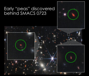
Vesoljski teleskop James Webb razkriva povezave med bližnjimi in daljnimi galaksijami
Izvorno vozlišče: 1889333
Časovni žig: Jan 9, 2023
Sprostitev nove dobe barvno nastavljivih nano naprav – najmanjši vir svetlobe s preklopljivimi oblikovanimi barvami
Izvorno vozlišče: 2801585
Časovni žig: Avgust 3, 2023
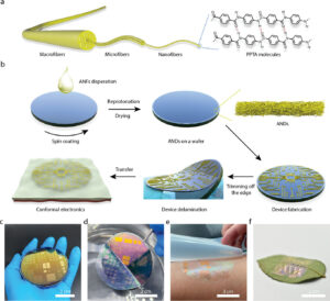
Nova ultra-tanka "koža" za prilagodljivo elektroniko obljublja napredek za medicinske pripomočke in protetiko
Izvorno vozlišče: 3075264
Časovni žig: Jan 20, 2024
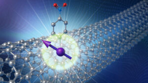
Ogljikove nanocevke so idealen dom za vrtenje kvantnih bitov
Izvorno vozlišče: 1995470
Časovni žig: Marec 6, 2023
Tok ubere presenetljivo pot v kvantnem materialu
Izvorno vozlišče: 2801583
Časovni žig: Avgust 3, 2023
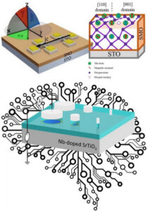
Kompleksni oksidi bi lahko poganjali računalnike prihodnosti
Izvorno vozlišče: 1997462
Časovni žig: Marec 7, 2023
Nenavaden atom pomaga pri iskanju gradnikov vesolja
Izvorno vozlišče: 1980749
Časovni žig: Februar 24, 2023
Prva univerzalna metapovršinska antena na svetu za visokovarne komunikacije 6G
Izvorno vozlišče: 3013617
Časovni žig: December 14, 2023