Новости: микроэлектроника
24 мая 2023
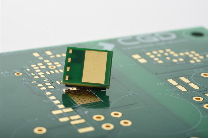
Cambridge GaN Devices Ltd (CGD) — which was spun out of the University of Cambridge Department of Engineering’s Electrical Power and Energy Conversion group in 2016 and designs, develops and commercializes power transistors and ICs that use GaN-on-silicon substrates — has introduced a range of Application Interface Boards that allow designers to try out its ICeGaN high-electron-mobility transistors (HEMTs) in existing circuits in place of competing MOSFET or GaN devices without having to re-layout the PCB.
Application Interface Boards are adaptor PCBs that are soldered to an ICeGaN device, which map each pin/signal from the ICeGaN HEMT footprint to the corresponding pins/signals of an alternative component footprint.
“These Application Interface Boards are designed for design and evaluation purposes only, of course. This is a quick, first step to enable the user to put one of our ICeGaN ICs into an existing design,” says Peter Comiskey, director of application engineering. “There is some minor impact on thermal performance, but surprisingly little difference in EMC or electrical performance.”
CGD offers Application Interface Boards for a number of industry-standard devices from leading MOSFET and GaN device makers. A full list can be found on the гид пользователя, but the firm can also develop an Application Interface Board for devices not currently supported for delivery within four weeks.
ICeGaN HEMT компании CGD доступны в больших объемах
- SEO-контент и PR-распределение. Получите усиление сегодня.
- ПлатонАйСтрим. Анализ данных Web3. Расширение знаний. Доступ здесь.
- Чеканка будущего с Эдриенн Эшли. Доступ здесь.
- Покупайте и продавайте акции компаний PREIPO® с помощью PREIPO®. Доступ здесь.
- Источник: https://www.semiconductor-today.com/news_items/2023/may/cgd-240523.shtml
- :имеет
- :является
- :нет
- 2016
- a
- позволять
- Также
- альтернатива
- an
- и
- Применение
- МЫ
- доступен
- BE
- доска
- но
- Кембридж
- CAN
- конкурирующий
- компонент
- Конверсия
- соответствующий
- курс
- В настоящее время
- поставка
- Кафедра
- Проект
- предназначенный
- дизайнеры
- конструкций
- развивать
- развивается
- устройство
- Устройства
- разница
- директор
- каждый
- включить
- энергетика
- Проект и
- оценка
- существующий
- Фирма
- First
- след
- Что касается
- найденный
- 4
- от
- полный
- группы
- имеющий
- High
- HTTP
- HTTPS
- ICS
- Влияние
- in
- Интерфейс
- в
- выпустили
- Представляет
- пункты
- ЕГО
- JPG
- ведущий
- Список
- мало
- ООО
- Makers
- карта
- Май..
- небольшая
- номер
- of
- Предложения
- on
- ONE
- только
- or
- наши
- внешний
- Печатные платы
- производительность
- Питер
- Часть
- Платон
- Платон Интеллектуальные данные
- ПлатонДанные
- мощностью
- целей
- положил
- САЙТ
- ассортимент
- Связанный
- говорит
- некоторые
- вращаться
- Шаг
- Поддержанный
- который
- Ассоциация
- тепловой
- этой
- в
- стараться
- Университет
- университет Кембриджа
- использование
- Информация о пользователе
- законопроект
- Недели
- который
- в
- без
- зефирнет