News: Suppliers
17 January 2023
k-Space Associates Inc of Dexter, MI, USA – which was founded in 1992 and produces thin-film metrology instrumentation and software for research and manufacturing of microelectronic, optoelectronic and photovoltaic devices – has launched the kSA XRF x-ray fluorescence thin-film metrology tool, which measures film thickness for materials that are too thin for reliable optical measurements.
The kSA XRF uses an x-ray source, detector and proprietary software to measure the x-ray emission spectrum, which is then used to calculate film thickness in real-time. It measures the appropriate atomic species based on the customer’s unique coating formula and measurement needs. This technique has been proven to measure semiconductor and dielectric layers on glass panels, wafers and susceptors for applications in solar, power, and other thin-film devices.
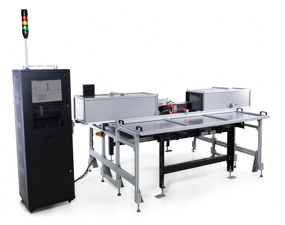
Picture: The kSA XRF, which can be configured for a standalone benchtop setup or over a conveyor for in-line inspection and manufacturing process control (as shown here).
“We developed the kSA XRF while helping one of our existing customers measure dielectric coatings that couldn’t be measured using traditional optical methods,” says CEO Darryl Barlett. “The XRF measures dielectric coatings below 100nm and can be used by makers of glass panels, solar panels, MOCVD [metal-organic chemical vapor deposition] carriers and other products,” he adds. “It’s a superior and more scalable option than existing tools and is easily installed into conveyor lines.”
The kSA XRF can be configured for a standalone benchtop setup or over a conveyor for in-line inspection and manufacturing process control.
“The kSA XRF allows users to characterize and monitor their thin-film coatings during production, thereby increasing yield and reducing costs,” notes Barlett.
- SEO Powered Content & PR Distribution. Get Amplified Today.
- Platoblockchain. Web3 Metaverse Intelligence. Knowledge Amplified. Access Here.
- Source: https://www.semiconductor-today.com/news_items/2023/jan/kspace-170123.shtml
- a
- Adds
- allows
- and
- applications
- appropriate
- based
- below
- carriers
- ceo
- characterize
- chemical
- control
- Costs
- Customers
- Darryl
- developed
- Devices
- during
- easily
- emission
- existing
- Film
- formula
- Founded
- glass
- helping
- here
- HTTPS
- in
- increasing
- IT
- January
- launched
- launches
- layers
- lines
- Makers
- manufacturing
- materials
- measure
- measurements
- measures
- methods
- Metrology
- Monitor
- more
- needs
- Notes
- ONE
- Option
- Other
- panels
- plato
- Plato Data Intelligence
- PlatoData
- power
- process
- Production
- Products
- proprietary
- proven
- real-time
- reducing
- reliable
- research
- scalable
- semiconductor
- setup
- shown
- Software
- solar
- solar panels
- Source
- Spectrum
- standalone
- superior
- The
- their
- thereby
- to
- too
- tool
- tools
- traditional
- unique
- USA
- users
- which
- while
- x-ray
- Yield
- zephyrnet