17 年 2023 月 XNUMX 日 (Nanowerkニュース) 私たちはデータの洪水の時代に生きています。この大量のデータを保存および処理するために運営されているデータセンターは大量の電力を使用しており、これが環境汚染の主な原因であると言われています。この状況を打開するために、消費電力が低く、計算速度が速いポリゴンコンピューティングシステムが研究されていますが、従来のバイナリコンピューティングシステムと同様に電気信号で動作するため、膨大なデータ処理需要に対応できません。
研究者らは、光パルスによって駆動される光メモリとして機能できる新しい2D-0D半導体材料を開発した。
この材料は複数の抵抗状態を可能にし、従来のメモリのように 0 と 1 の状態以上の状態を可能にします。
これにより、システムのコンピューティング部分とストレージ部分の間の高速光データ伝送が可能になる可能性があります。
テストでは、光メモリは AI モデルで 91% の精度を達成し、次世代コンピューティングの可能性を示しました。
研究者らは、これがAIやその他の先進システムにおけるシリコン半導体の限界を克服するのに役立つ可能性があると述べている。
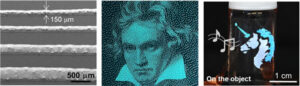
 2D-0D ハイブリッド光メモリ デバイス。 (画像:KIST)
主要な取り組み
2D-0D ハイブリッド光メモリ デバイス。 (画像:KIST)
リサーチ
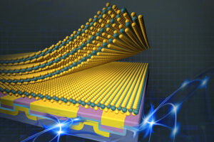
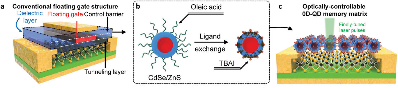
韓国科学技術研究院(KIST)は、光電子材料デバイスセンターのド・ギョン・ファン博士と大邱慶北科学技術大学エネルギー科学工学科のイ・ジョンス教授が研究成果を発表したと発表した( DGIST) は、新しいゼロ次元および二次元 (2D-0D) 半導体人工接合材料を共同開発し、光を動力源とする次世代メモリの効果を観察しました。電気信号ではなく光を使用してマルチレベル コンピューターの計算部分と記憶部分の間でデータを送信すると、処理速度が大幅に向上します。この研究は、 先端材料 (“Probing optical multi-level memory effects in single core-shell quantum dots and application through 2D-0D hybrid inverters”)。研究チームは、接合により新しい2D-0D半導体人工接合材料を作製した 量子ドット セレン化カドミウム(CdSe)と硫化モリブデン(MoS)の表面に硫化亜鉛(ZnS)を配したコアシェル構造となっています。2) semiconductor. The new material enables the storage and manipulation of electronic states within quantum dots measuring 10 nm or less. When light is applied to the cadmium selenide core, a certain number of electrons flow out of the molybdenum sulfide semiconductor, trapping holes in the core and making it conductive. The electron state inside cadmium selenide is also quantized. Intermittent light pulses trap electrons in the electron band one after the other, inducing a change in the resistance of the molybdenum sulfide through the field effect, and the resistance changes in a cascading manner depending on the number of light pulses. This process makes it possible to divide and maintain more than 0 and 10 states, unlike conventional memory, which has only 0 and 1 states. The zinc sulfide shell also prevents charge leakage between neighboring quantum dots, allowing each single quantum dot to function as a memory. While quantum dots in conventional 2D-0D semiconductor artificial junction structures simply amplify signals from light sensors, the team’s quantum dot structure perfectly mimics the floating gate memory structure, confirming its potential for use as a next-generation optical memory. The researchers verified the effectiveness of the polynomial memory phenomenon with neural network modeling using the CIFAR-10 dataset and achieved a 91% recognition rate. Dr. Hwang of KIST said, “The new multi-level optical memory device will contribute to accelerating the industrialization of next-generation system technologies such as artificial intelligence systems, which have been difficult to commercialize due to technical limitations arising from the miniaturization and integration of existing silicon semiconductor devices.”- SEO を活用したコンテンツと PR 配信。 今日増幅されます。
- PlatoData.Network 垂直生成 Ai。 自分自身に力を与えましょう。 こちらからアクセスしてください。
- プラトアイストリーム。 Web3 インテリジェンス。 知識増幅。 こちらからアクセスしてください。
- プラトンESG。 カーボン、 クリーンテック、 エネルギー、 環境、 太陽、 廃棄物管理。 こちらからアクセスしてください。
- プラトンヘルス。 バイオテクノロジーと臨床試験のインテリジェンス。 こちらからアクセスしてください。
- 情報源: https://www.nanowerk.com/nanotechnology-news2/newsid=63861.php
- :持っている
- :は
- :not
- 1
- 10
- 17
- 7
- 8
- 9
- a
- できる
- 加速している
- 精度
- 達成
- 高度な
- 後
- AI
- 許可
- ことができます
- また
- 増幅する
- an
- および
- 発表の
- 申し込み
- 適用された
- です
- 人工の
- 人工知能
- AS
- At
- BAND
- なぜなら
- き
- さ
- の間に
- 焙煎が極度に未発達や過発達のコーヒーにて、クロロゲン酸の味わいへの影響は強くなり、金属を思わせる味わいと乾いたマウスフィールを感じさせます。
- by
- 呼ばれます
- 缶
- センター
- センター
- 一定
- 変化する
- 変更
- チャージ
- 商品化
- 計算
- コンピュータ
- コンピューティング
- 消費
- 貢献する
- 寄稿者
- 従来の
- 基本
- 可能性
- データ
- データセンター
- データ処理
- 日付
- 需要
- 部門
- エネルギー省
- によっては
- 発展した
- デバイス
- Devices
- 難しい
- 分割
- do
- DOT
- dr
- 劇的に
- 原因
- 各
- 効果
- 有効
- 効果
- 電気
- エレクトロニック
- 電子
- enable
- 可能
- 有効にする
- エネルギー
- エンジニアリング
- 環境の
- 時代
- エーテル(ETH)
- 既存の
- フィールド
- floating
- 洪水
- フロー
- から
- function
- ハンドル
- 持ってる
- 助けます
- より高い
- 穴
- HTTPS
- 巨大な
- ハイブリッド
- 画像
- in
- 増える
- 内部
- 機関
- 統合
- インテリジェンス
- IT
- ITS
- 参加
- JPG
- ただ
- 韓国
- リー
- less
- 光
- ような
- 制限
- ライブ
- たくさん
- 下側
- 維持する
- 主要な
- 作る
- 作成
- 操作
- 方法
- 材料
- 材料
- 計測
- 思い出
- メモリ
- 真ん中
- モデリング
- 他には?
- の試合に
- 近所の
- ネットワーク
- ニューラル
- ニューラルネットワーク
- 新作
- 次世代
- 数
- 観測された
- of
- on
- ONE
- の
- 操作する
- 運営
- or
- その他
- でる
- 克服する
- 部品
- 完璧に
- 現象
- PHP
- プラトン
- プラトンデータインテリジェンス
- プラトデータ
- 汚染
- 可能
- 潜在的な
- 電力
- パワード
- を防止
- プロセス
- 処理
- 東京大学大学院海洋学研究室教授
- 約束
- 公表
- 量子
- 量子ドット
- 量子ドット
- レート
- むしろ
- 認識
- 研究
- 研究者
- s
- 前記
- 言う
- 科学
- 科学技術
- 半導体
- 半導体関連装置
- センサー
- シェル(Shell)
- 表示
- 信号
- シリコン
- 単に
- 状況
- スピード
- 都道府県
- 米国
- ストレージ利用料
- 店舗
- 構造
- 構造
- そのような
- 表面
- システム
- チーム
- 技術的
- テクノロジー
- テクノロジー
- テスト
- より
- それ
- 彼ら
- この
- 介して
- 〜へ
- トラッピング
- 異なり、
- つかいます
- 案内
- 検証
- we
- いつ
- which
- while
- 意志
- 以内
- ゼファーネット