08年2023月XNUMX日(Nanowerkニュース) Researchers at Columbia Engineering have developed a new class of integrated photonic devices–“leaky-wave metasurfaces”–that can convert light initially confined in an optical waveguide to an arbitrary optical pattern in free space (自然ナノテクノロジー, “Leaky-wave metasurfaces for integrated photonics”).
These devices are the first to demonstrate simultaneous control of all four optical degrees of freedom, namely, amplitude, phase, polarization ellipticity, and polarization orientation–a world record. Because the devices are so thin, transparent, and compatible with photonic integrated circuits (PICs), they can be used to improve optical displays, LIDAR (Light Detection and Ranging), optical communications, and quantum optics.
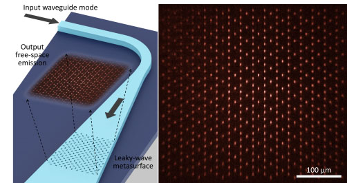 Figure 1. Left: Schematic showing the operation of a leaky-wave metasurface. Right: A 2D array of optical spots forming a Kagome pattern that is produced by a leaky-wave metasurface. (Image: Heqing Huang, Adam Overvig, and Nanfang Yu/Columbia Engineering)
“We are excited to find an elegant solution for interfacing free-space optics and integrated photonics–these two platforms have traditionally been studied by investigators from different subfields of optics and have led to commercial products addressing completely different needs,” said Nanfang Yu, associate professor of applied physics and applied mathematics who is a leader in research on nanophotonic devices. “Our work points to new ways to create hybrid systems that utilize the best of both worlds–free-space optics for shaping the wavefront of light and integrated photonics for optical data processing–to address many emerging applications such as quantum optics, optogenetics, sensor networks, inter-chip communications, and holographic displays.”
Figure 1. Left: Schematic showing the operation of a leaky-wave metasurface. Right: A 2D array of optical spots forming a Kagome pattern that is produced by a leaky-wave metasurface. (Image: Heqing Huang, Adam Overvig, and Nanfang Yu/Columbia Engineering)
“We are excited to find an elegant solution for interfacing free-space optics and integrated photonics–these two platforms have traditionally been studied by investigators from different subfields of optics and have led to commercial products addressing completely different needs,” said Nanfang Yu, associate professor of applied physics and applied mathematics who is a leader in research on nanophotonic devices. “Our work points to new ways to create hybrid systems that utilize the best of both worlds–free-space optics for shaping the wavefront of light and integrated photonics for optical data processing–to address many emerging applications such as quantum optics, optogenetics, sensor networks, inter-chip communications, and holographic displays.”
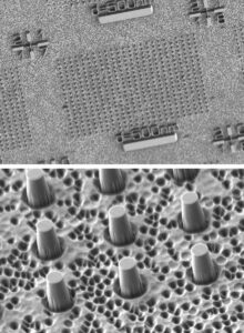
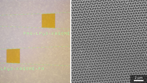 図 2. 左: カゴメ格子を生成するための XNUMX つの漏洩波メタ表面の写真。右: 漏洩波メタ表面の一部の SEM 画像。窒化ケイ素薄膜上のポリマー層にエッチングされたナノ開口で構成されます。 (画像: Heqing Huang、Adam Overvig、Nanfang Yu/Columbia Engineering)
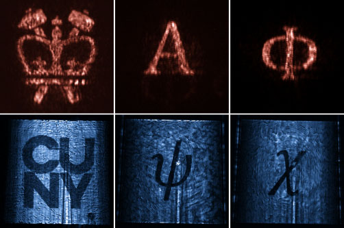 図 3. 左の XNUMX つの図: デバイス表面から XNUMX つの異なる距離にある漏洩波メタ表面によって生成された XNUMX つのホログラフィック イメージ。右の XNUMX つの図: デバイス表面から XNUMX つの異なる距離にあり、XNUMX つの直交する偏光状態で、単一の漏洩波メタ表面によって生成された XNUMX つの異なるホログラフィック イメージ。 (画像: Heqing Huang、Adam Overvig、Nanfang Yu/Columbia Engineering)
Figure 1. Left: Schematic showing the operation of a leaky-wave metasurface. Right: A 2D array of optical spots forming a Kagome pattern that is produced by a leaky-wave metasurface. (Image: Heqing Huang, Adam Overvig, and Nanfang Yu/Columbia Engineering)
“We are excited to find an elegant solution for interfacing free-space optics and integrated photonics–these two platforms have traditionally been studied by investigators from different subfields of optics and have led to commercial products addressing completely different needs,” said Nanfang Yu, associate professor of applied physics and applied mathematics who is a leader in research on nanophotonic devices. “Our work points to new ways to create hybrid systems that utilize the best of both worlds–free-space optics for shaping the wavefront of light and integrated photonics for optical data processing–to address many emerging applications such as quantum optics, optogenetics, sensor networks, inter-chip communications, and holographic displays.”
自由空間光学と統合フォトニクスの橋渡し
The key challenge of interfacing PICs and free-space optics is to transform a simple waveguide mode confined within a waveguide–a thin ridge defined on a chip–into a broad free-space wave with a complex wavefront, and vice versa. Yu’s team tackled this challenge by building on their invention last fall of “nonlocal metasurfaces” and extended the devices’ functionality from controlling free-space light waves to controlling guided waves. Specifically, they expanded the input waveguide mode by using a waveguide taper into a slab waveguide mode–a sheet of light propagating along the chip. “We realized that the slab waveguide mode can be decomposed into two orthogonal standing waves–waves reminiscent of those produced by plucking a string,” said Heqing Huang, a PhD student in Yu’s lab and co-first author of the study, published today in Nature Nanotechnology. “Therefore, we designed a ‘leaky-wave metasurface’ composed of two sets of rectangular apertures that have a subwavelength offset from each other to independently control these two standing waves. The result is that each standing wave is converted into a surface emission with independent amplitude and polarization; together, the two surface emission components merge into a single free-space wave with completely controllable amplitude, phase, and polarization at each point over its wavefront.”
図 2. 左: カゴメ格子を生成するための XNUMX つの漏洩波メタ表面の写真。右: 漏洩波メタ表面の一部の SEM 画像。窒化ケイ素薄膜上のポリマー層にエッチングされたナノ開口で構成されます。 (画像: Heqing Huang、Adam Overvig、Nanfang Yu/Columbia Engineering)
量子光学から光通信、ホログラフィック 3D ディスプレイまで
Yu氏のチームは複数の漏洩波を実験的に実証した メタサーフェス これは、300波長程度の断面積を持つ導波路に沿って伝播する導波路モードを、1.55ミクロンの通信波長で波長の約3倍の領域にわたる設計波面を持つ自由空間放射に変換できる。これらには次のものが含まれます。 自由空間に焦点を生成する漏洩波メタレンズ。このようなデバイスは、PIC チップ間に低損失、大容量の自由空間光リンクを形成するのに理想的です。また、プローブから遠く離れたニューロンを光学的に刺激するための集束ビームを生成する統合光遺伝学プローブにも役立ちます。 自由空間にカゴメ格子パターンを形成する数百の焦点を生成できる漏洩波光格子発生器。一般に、漏洩波メタ表面は、冷たい原子や分子を捕捉するために、複雑な非周期的かつ三次元の光格子を生成することができます。この機能により、研究者は、これまで他のプラットフォームでは容易に達成できなかったエキゾチックな量子光学現象を研究したり、量子シミュレーションを実行したりできるようになり、原子配列ベースの量子デバイスの複雑さ、体積、コストを大幅に削減できるようになります。たとえば、漏洩波メタ表面を真空チャンバに直接統合して光学システムを簡素化し、原子時計などのポータブル量子光学アプリケーションの可能性を高めることができます。 らせん状の波面を持つビームを生成する漏洩波渦ビーム発生器。これにより、PIC に依存して光によって運ばれる情報を処理すると同時に、大容量の相互通信のために成形された波面を持つ光波を使用する、建物間の自由空間光リンクが実現する可能性があります。 XNUMX つの異なる画像を同時に置き換えることができる漏洩波ホログラム。XNUMX つはデバイス面にあり (XNUMX つの直交する偏光状態にある)、もう XNUMX つは自由空間内の離れた場所にある (これも XNUMX つの直交する偏光状態にある)。この機能を使用すると、より軽量で快適な拡張現実ゴーグルや、よりリアルなホログラフィック XNUMXD ディスプレイを作成できる可能性があります。
図 3. 左の XNUMX つの図: デバイス表面から XNUMX つの異なる距離にある漏洩波メタ表面によって生成された XNUMX つのホログラフィック イメージ。右の XNUMX つの図: デバイス表面から XNUMX つの異なる距離にあり、XNUMX つの直交する偏光状態で、単一の漏洩波メタ表面によって生成された XNUMX つの異なるホログラフィック イメージ。 (画像: Heqing Huang、Adam Overvig、Nanfang Yu/Columbia Engineering)
デバイスの製造
デバイスの製造は、コロンビア ナノ イニシアチブのクリーンルームと、ニューヨーク市立大学大学院センターの先端科学研究センター ナノ製造施設で行われました。次のステップ
Yu 氏の現在のデモンストレーションは、近赤外波長での単純なポリマー窒化ケイ素材料プラットフォームに基づいています。彼のチームは次に、鋳造製造プロトコルと互換性があり、高光出力動作に耐えられる、より堅牢な窒化ケイ素プラットフォームに基づくデバイスを実証することを計画しています。また、量子光学やホログラフィックディスプレイなどの用途に適した、高い出力効率と可視波長での動作の設計を実証する予定だ。- SEO を活用したコンテンツと PR 配信。 今日増幅されます。
- プラトアイストリーム。 Web3 データ インテリジェンス。 知識増幅。 こちらからアクセスしてください。
- 未来を鋳造する w エイドリエン・アシュリー。 こちらからアクセスしてください。
- PREIPO® を使用して PRE-IPO 企業の株式を売買します。 こちらからアクセスしてください。
- 情報源: https://www.nanowerk.com/nanotechnology-news2/newsid=62957.php
- :は
- :not
- 1
- 10
- 11
- 13
- 2D
- 3d
- 7
- 8
- a
- 私たちについて
- アダム
- 住所
- アドレッシング
- 高度な
- すべて
- 沿って
- また
- an
- および
- 別の
- 適用された
- です
- AREA
- 配列
- AS
- 仲間
- At
- 達成できる
- 増強された
- 拡張現実
- 著者
- 離れて
- ベース
- BE
- ビーム
- なぜなら
- き
- BEST
- の間に
- 両言語で
- 広い
- 建物
- by
- 缶
- センター
- 挑戦する
- 室
- チップ
- チップ
- 市町村
- class
- 時計
- 冷たい
- Columbia
- 快適
- コマーシャル
- 通信部
- 互換性のあります
- 完全に
- 複雑な
- 複雑さ
- コンポーネント
- 構成
- プロフェッショナルな方法で
- コントロール
- 制御
- 変換
- 変換
- 費用
- 可能性
- 作ります
- 電流プローブ
- データ
- 日付
- 定義済みの
- 実証します
- 実証
- 設計
- デザイナー
- デザイン
- 検出
- 発展した
- デバイス
- Devices
- 異なります
- 直接に
- ディスプレイ
- 距離
- 明確な
- 各
- 簡単に
- 効率
- 新興の
- エミッション
- enable
- エンジニアリング
- 例
- 興奮した
- エキゾチック
- 拡大
- 施設
- 秋
- 遠く
- フィギュア
- 膜
- もう完成させ、ワークスペースに掲示しましたか?
- 名
- 焦点を当て
- ファウンドリ
- 4
- 無料版
- フリースペース
- 自由
- から
- function
- 機能性
- 生成
- ジェネレータ
- 卒業生
- 持ってる
- ハイ
- 彼の
- ホログラム
- ホログラフィック
- HTTPS
- 何百
- ハイブリッド
- 理想
- 画像
- 画像
- 改善します
- in
- include
- 独立しました
- 単独で
- 情報
- 当初
- イニシアチブ
- 統合された
- インタフェース
- に
- 発明
- 研究者
- IT
- ITS
- JPG
- キー
- ラボ
- 姓
- 層
- つながる
- リーダー
- ツェッペリン
- 左
- 対処
- 光
- ライター
- LINK
- 位置して
- make
- 作成
- 多くの
- 材料
- 数学
- マージ
- 真ん中
- モード
- 他には?
- の試合に
- すなわち
- ドワーフ
- ナノテクノロジー
- 自然
- ニーズ
- ネットワーク
- ニューロン
- 新作
- ニューヨーク
- 次の
- of
- オフセット
- on
- ONE
- 操作
- 光学
- or
- 注文
- その他
- でる
- 出力
- が
- パターン
- 完璧
- 相
- PHP
- 物理学
- 計画
- プラン
- プラットフォーム
- プラットフォーム
- プラトン
- プラトンデータインテリジェンス
- プラトデータ
- ポイント
- ポイント
- ポリマー
- 可能性
- 電力
- プローブ
- プロセス
- 作り出す
- 生産された
- 製品
- 東京大学大学院海洋学研究室教授
- プロトコル
- 公表
- 量子
- 量子光学
- 測距
- 現実的な
- 現実
- 実現
- 記録
- 減らします
- 連想させます
- 研究
- 研究者
- 結果
- 堅牢な
- 前記
- 科学
- SEM
- セット
- 形
- シェーピング
- シリコン
- 簡単な拡張で
- 簡素化する
- 同時
- 同時に
- So
- 溶液
- スペース
- 特に
- Spot
- 米国
- 文字列
- 学生
- 研究
- 勉強
- 実質上
- そのような
- 適当
- 表面
- システム
- チーム
- 電気通信
- それ
- アプリ環境に合わせて
- それら
- ボーマン
- 彼ら
- この
- それらの
- 三次元の
- <font style="vertical-align: inherit;">回数</font>
- 〜へ
- 今日
- 一緒に
- top
- 伝統的に
- 最適化の適用
- トランスペアレント
- 2
- 大学
- 中古
- 活用する
- 目に見える
- ボリューム
- ました
- ウェーブ
- 波長
- 波浪
- 方法
- we
- which
- while
- 誰
- 意志
- 以内
- 仕事
- 世界
- ヨーク
- ゼファーネット