יאן 24, 2024
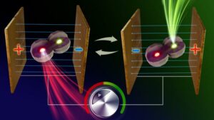
(חדשות Nanowerk) Researchers with the Department of Energy’s SLAC National Accelerator Laboratory, Stanford University and the DOE’s Lawrence Berkeley National Laboratory (LBNL) grew a twisted multilayer crystal structure for the first time and measured the structure’s key properties. The twisted structure could help researchers develop next-generation materials for solar cells, quantum computers, lasers and other devices.
“This structure is something that we have not seen before – it was a huge surprise to me,” said Yi Cui, a professor at Stanford and SLAC and paper co-author. “A new quantum electronic property could appear within this three-layer twisted structure in future experiments.”
 כּוֹתֶרֶת
הוספת שכבות, עם טוויסט
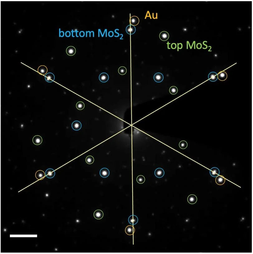
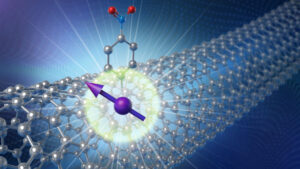
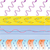
The crystals the team designed extended the concept of epitaxy, a phenomenon that occurs when one type of crystal material grows on top of another material in an ordered way – kind of like growing a neat lawn on top of soil, but at the atomic level. Understanding epitaxial growth has been critical to the development of many industries for more than 50 years, particularly the semiconductor industry. Indeed, epitaxy is part of many of the electronic devices that we use today, from cell phones to computers to solar panels, allowing electricity to flow, and not flow, through them. To date, epitaxy research has focused on growing one layer of material onto another, and the two materials have the same crystal orientation at the interface. This approach has been successful for decades in many applications, such as transistors, light-emitting diodes, lasers and quantum devices. But to find new materials that perform even better for more demanding needs, like quantum computing, researchers are searching for other epitaxial designs – ones that might be more complex, yet better performing, hence the “twisted epitaxy” concept demonstrated in this study. In their experiment, detailed in מדע (“Twisted epitaxy of gold nanodisks grown between twisted substrate layers of molybdenum disulfide”), הוסיפו חוקרים שכבה של זהב בין שתי יריעות של חומר מוליך למחצה מסורתי, מוליבדן דיסולפיד (MoS2). Because the top and bottom sheets were oriented differently, the gold atoms could not align with both simultaneously, which allowed the Au structure to twist, said Yi Cui, Professor Cui’s graduate student in materials science and engineering at Stanford and co-author of the paper. “With only a bottom MoS2 שכבה, הזהב שמח להתיישר איתה, אז שום טוויסט לא קורה", אמר קוי, הסטודנט לתואר שני. "אבל עם שני MoS מעוותים2 גיליונות, הזהב לא בטוח מיושר עם השכבה העליונה או התחתונה. הצלחנו לעזור לזהב לפתור את הבלבול שלו וגילינו קשר בין הכיוון של Au לזווית הפיתול של MoS דו-שכבתי2".ננו-דיסקיות זהב לזוז
כדי לחקור את שכבת הזהב בפירוט, צוות החוקרים ממכון סטנפורד למדעי החומרים והאנרגיה (SIMES) ו-LBNL חיממו דגימה של המבנה כולו ל-500 מעלות צלזיוס. לאחר מכן הם שלחו זרם של אלקטרונים דרך הדגימה באמצעות טכניקה הנקראת מיקרוסקופ אלקטרונים העברה (TEM), שחשפה את המורפולוגיה, הכיוון והמתח של ננו-דיסקיות הזהב לאחר חישול בטמפרטורות שונות. מדידת המאפיינים הללו של ננו-דיסקים מזהב הייתה צעד ראשון הכרחי לקראת ההבנה כיצד ניתן לתכנן את המבנה החדש עבור יישומים בעולם האמיתי בעתיד. "ללא המחקר הזה, לא היינו יודעים אם פיתול שכבת מתכת אפיטקסיאלית על גבי מוליך למחצה בכלל אפשרי", אמר Cui, הסטודנט לתואר שני. "מדידה של המבנה התלת-שכבתי המלא במיקרוסקופ אלקטרוני אישרה שזה לא רק אפשרי, אלא גם שניתן לשלוט במבנה החדש בדרכים מרגשות". בשלב הבא, החוקרים רוצים להמשיך ולחקור את המאפיינים האופטיים של ננו-דיסקיות הזהב באמצעות TEM וללמוד אם העיצוב שלהם משנה מאפיינים פיזיים כמו מבנה הלהקה של Au. הם גם רוצים להרחיב את הרעיון הזה כדי לנסות לבנות מבנים תלת-שכבתיים עם חומרים מוליכים למחצה אחרים ומתכות אחרות. "אנחנו מתחילים לחקור אם רק שילוב זה של חומרים מאפשר זאת או אם זה קורה בצורה רחבה יותר," אמר בוב סינקלייר, פרופסור צ'ארלס מ. פיגוט בבית הספר למדעים והנדסת חומרים בסטנפורד ומחבר שותף במאמר. "הגילוי הזה פותח סדרה חדשה לגמרי של ניסויים שאנחנו יכולים לנסות. אנחנו יכולים להיות בדרך למצוא תכונות חומר חדשות שנוכל לנצל".- הפצת תוכן ויחסי ציבור מופעל על ידי SEO. קבל הגברה היום.
- PlatoData.Network Vertical Generative Ai. העצים את עצמך. גישה כאן.
- PlatoAiStream. Web3 Intelligence. הידע מוגבר. גישה כאן.
- PlatoESG. פחמן, קלינטק, אנרגיה, סביבה, שמש, ניהול פסולת. גישה כאן.
- PlatoHealth. מודיעין ביוטכנולוגיה וניסויים קליניים. גישה כאן.
- מקור: https://www.nanowerk.com/nanotechnology-news3/newsid=64500.php
- :יש ל
- :הוא
- :לֹא
- 10
- 13
- 14
- 24
- 50
- 50 שנים
- 500
- 7
- 8
- 9
- a
- מאיץ
- להוסיף
- הוסיף
- לאחר
- ליישר
- מותר
- מאפשר
- מאפשר
- גם
- an
- ו
- אחר
- לְהוֹפִיעַ
- יישומים
- גישה
- ARE
- AS
- At
- אטומי
- להקה
- BE
- כי
- היה
- לפני
- ההתחלה
- ברקלי
- מוטב
- בֵּין
- שילינג
- שניהם
- תַחתִית
- מותג
- חדש
- בְּהַרְחָבָה
- לִבנוֹת
- אבל
- נקרא
- CAN
- תא
- טלפון נייד
- תאים
- צֶלסִיוּס
- מרכז
- צ'ארלס
- מחבר שותף
- שילוב
- להשלים
- מורכב
- מחשבים
- מחשוב
- מושג
- מְאוּשָׁר
- בלבול
- נשלט
- יכול
- קריטי
- גָבִישׁ
- תַאֲרִיך
- עשרות שנים
- תובעני
- מופגן
- מַחלָקָה
- עיצוב
- מעוצב
- עיצובים
- פרט
- מְפוֹרָט
- לפתח
- צעצועי התפתחות
- התקנים
- אחר
- באופן שונה
- גילה
- תגלית
- DOE
- חשמל
- אֶלֶקטרוֹנִי
- אלקטרונים
- אנרגיה
- הנדסה
- אֲפִילוּ
- מרגש
- לְנַסוֹת
- ניסויים
- לנצל
- לחקור
- להאריך
- מוּרחָב
- מציאת
- ראשון
- firsttime
- תזרים
- מרוכז
- בעד
- החל מ-
- נוסף
- עתיד
- זהב
- בוגר
- גדלתי
- גדל
- מְגוּדָל
- גדל
- צמיחה
- קורה
- שמח
- יש
- לעזור
- ומכאן
- איך
- HTTPS
- עצום
- if
- תמונה
- in
- תעשיות
- תעשייה
- מכון
- מִמְשָׁק
- IT
- שֶׁלָה
- jpg
- מפתח
- סוג
- לדעת
- מעבדה
- לייזרים
- לורנס
- שכבה
- שכבות
- לִלמוֹד
- רמה
- כמו
- הצליח
- רב
- חוֹמֶר
- עיצוב חומר
- חומרים
- me
- נמדד
- מדידת
- מתכת
- מתכות
- מיקרוסקופיה
- אמצע
- יכול
- יותר
- לאומי
- נקי
- הכרחי
- צרכי
- חדש
- הבא
- הדור הבא
- לא
- of
- on
- ONE
- יחידות
- רק
- פתיחה
- or
- אחר
- שלנו
- פנלים
- מאמר
- חלק
- במיוחד
- לבצע
- ביצוע
- תופעה
- טלפונים
- גופני
- אפלטון
- מודיעין אפלטון
- אפלטון נתונים
- אפשרי
- פרופסור
- נכסים
- רכוש
- קוונטית
- מחשבים קוונטיים
- מחשוב קוונטי
- ממשי
- עולם אמיתי
- קשר
- מחקר
- חוקר
- חוקרים
- גילה
- s
- אמר
- אותו
- בית ספר
- מדע
- מדעים
- חיפוש
- לראות
- סמיקונדקטור
- נשלח
- סדרה
- גיליונות
- בו זמנית
- So
- אדמה
- סולרי
- תאים סולאריים
- פנלים סולאריים
- לפתור
- משהו
- סטנפורד
- אוניברסיטת סטנפורד
- שלב
- זרם
- מִבְנֶה
- מבנים
- סטודנט
- לימוד
- מוצלח
- כזה
- בטוח
- הפתעה
- נבחרת
- טכניקה
- טֶקסט
- מֵאֲשֶׁר
- זֶה
- השמיים
- העתיד
- שֶׁלָהֶם
- אותם
- אז
- אלה
- הֵם
- זֶה
- דרך
- זמן
- ל
- היום
- חלק עליון
- לקראת
- מסורתי
- לנסות
- לפתול
- שתיים
- סוג
- הבנה
- אוניברסיטה
- להשתמש
- באמצעות
- רוצה
- היה
- דֶרֶך..
- דרכים
- we
- היו
- מתי
- אם
- אשר
- כל
- עם
- בתוך
- עוֹלָם
- היה
- שנים
- עוד
- זפירנט
עוד מ ננוווק
חוקרים פיתחו שיטת הרכבה עצמית חדשה לייצור ננו-דפי-ממד רב-שכבתיים
צומת המקור: 3088801
בול זמן: יאן 29, 2024
'סנדוויץ' מסוים של גרפן ובורון ניטריד עשוי להוביל למיקרו-אלקטרוניקה מהדור הבא
צומת המקור: 2598354
בול זמן: אפריל 20, 2023
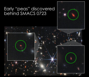
טלסקופ החלל ג'יימס ווב חושף קשרים בין גלקסיות קרובות ורחוקות
צומת המקור: 1889333
בול זמן: יאן 9, 2023
שחרור עידן חדש של מכשירי ננו הניתנים לכוונון צבע - מקור האור הקטן ביותר אי פעם עם צבעים ניתנים להחלפה שנוצרו
צומת המקור: 2801585
בול זמן: אוגוסט 3, 2023
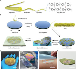
'עור' חדש דק במיוחד עבור אלקטרוניקה גמישה מבטיח התקדמות עבור מכשירים רפואיים ותותבות
צומת המקור: 3075264
בול זמן: יאן 20, 2024
האנטנה המטה-משטחית האוניברסלית הראשונה בעולם לתקשורת 6G ברמת אבטחה גבוהה
צומת המקור: 3013617
בול זמן: דצמבר 14, 2023