Jan 24, 2024
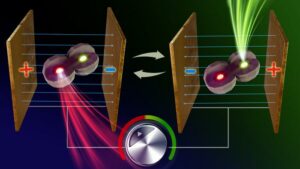
(Nanowerki uudised) Researchers with the Department of Energy’s SLAC National Accelerator Laboratory, Stanford University and the DOE’s Lawrence Berkeley National Laboratory (LBNL) grew a twisted multilayer crystal structure for the first time and measured the structure’s key properties. The twisted structure could help researchers develop next-generation materials for solar cells, quantum computers, lasers and other devices.
“This structure is something that we have not seen before – it was a huge surprise to me,” said Yi Cui, a professor at Stanford and SLAC and paper co-author. “A new quantum electronic property could appear within this three-layer twisted structure in future experiments.”
 RAKENDAMINE
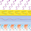
Kihtide lisamine, keeramisega
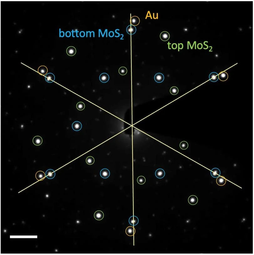
The crystals the team designed extended the concept of epitaxy, a phenomenon that occurs when one type of crystal material grows on top of another material in an ordered way – kind of like growing a neat lawn on top of soil, but at the atomic level. Understanding epitaxial growth has been critical to the development of many industries for more than 50 years, particularly the semiconductor industry. Indeed, epitaxy is part of many of the electronic devices that we use today, from cell phones to computers to solar panels, allowing electricity to flow, and not flow, through them. To date, epitaxy research has focused on growing one layer of material onto another, and the two materials have the same crystal orientation at the interface. This approach has been successful for decades in many applications, such as transistors, light-emitting diodes, lasers and quantum devices. But to find new materials that perform even better for more demanding needs, like quantum computing, researchers are searching for other epitaxial designs – ones that might be more complex, yet better performing, hence the “twisted epitaxy” concept demonstrated in this study. In their experiment, detailed in teadus (“Twisted epitaxy of gold nanodisks grown between twisted substrate layers of molybdenum disulfide”), lisasid teadlased kahe traditsioonilise pooljuhtmaterjali, molübdeendisulfiidi (MoS) lehe vahele kullakihi.2). Because the top and bottom sheets were oriented differently, the gold atoms could not align with both simultaneously, which allowed the Au structure to twist, said Yi Cui, Professor Cui’s graduate student in materials science and engineering at Stanford and co-author of the paper. “With only a bottom MoS2 kiht, joondub kuld sellega hea meelega, nii et väänamist ei juhtu,” ütles kraadiõppur Cui. "Aga kahe keerutatud MoS-iga2 lehed, ei ole kuld kindlasti ülemise või alumise kihiga joondatud. Meil õnnestus aidata kullal selle segadust lahendada ja avastasime seose Au orientatsiooni ja kahekihilise MoS-i pöördenurga vahel2. "Kuldsed nanokettad
Kullakihi üksikasjalikuks uurimiseks kuumutasid Stanfordi Materjali- ja Energiateaduste Instituudi (SIMES) ja LBNL teadlaste meeskond kogu struktuuri proovi 500 kraadini Celsiuse järgi. Seejärel saatsid nad proovi kaudu elektronide voo, kasutades tehnikat, mida nimetatakse transmissioonielektronmikroskoopiaks (TEM), mis näitas kulla nanodiskide morfoloogiat, orientatsiooni ja tüve pärast lõõmutamist erinevatel temperatuuridel. Kuld-nanodiskide nende omaduste mõõtmine oli vajalik esimene samm, et mõista, kuidas uut struktuuri saaks tulevikus reaalses maailmas kasutada. "Ilma selle uuringuta ei teaks me, kas epitaksiaalse metallikihi keeramine pooljuhi peale on üldse võimalik," ütles kraadiõppur Cui. "Täieliku kolmekihilise struktuuri mõõtmine elektronmikroskoopiaga kinnitas, et see pole mitte ainult võimalik, vaid ka seda, et uut struktuuri saab põnevatel viisidel juhtida." Järgmisena soovivad teadlased TEM-i abil täiendavalt uurida kulla nanoketaste optilisi omadusi ja teada saada, kas nende disain muudab füüsilisi omadusi, nagu Au riba struktuur. Samuti soovivad nad seda kontseptsiooni laiendada, et proovida ehitada kolmekihilisi struktuure teiste pooljuhtmaterjalide ja muude metallidega. "Hakkame uurima, kas ainult see materjalide kombinatsioon võimaldab seda või juhtub see laiemalt," ütles Bob Sinclair, Charles M. Pigotti professor Stanfordi materjaliteaduse ja tehnika koolist ning paberi kaasautor. "See avastus avab täiesti uue katsete seeria, mida saame proovida. Võiksime olla teel, et leida täiesti uusi materjaliomadusi, mida saaksime ära kasutada.- SEO-põhise sisu ja PR-levi. Võimenduge juba täna.
- PlatoData.Network Vertikaalne generatiivne Ai. Jõustage ennast. Juurdepääs siia.
- PlatoAiStream. Web3 luure. Täiustatud teadmised. Juurdepääs siia.
- PlatoESG. Süsinik, CleanTech, Energia, Keskkond päikeseenergia, Jäätmekäitluse. Juurdepääs siia.
- PlatoTervis. Biotehnoloogia ja kliiniliste uuringute luureandmed. Juurdepääs siia.
- Allikas: https://www.nanowerk.com/nanotechnology-news3/newsid=64500.php
- :on
- :on
- :mitte
- 10
- 13
- 14
- 24
- 50
- 50 aastat
- 500
- 7
- 8
- 9
- a
- kiirendi
- lisama
- lisatud
- pärast
- viia
- lubatud
- Lubades
- võimaldab
- Ka
- an
- ja
- Teine
- ilmuma
- rakendused
- lähenemine
- OLEME
- AS
- At
- aatomi-
- BAND
- BE
- sest
- olnud
- enne
- Algus
- Berkeley
- Parem
- vahel
- tera
- mõlemad
- põhi
- bränd
- Brand New
- üldjoontes
- ehitama
- kuid
- kutsutud
- CAN
- rakk
- Mobiiltelefonid
- Rakke
- Celsius
- keskus
- Charles
- Kaasautor
- kombinatsioon
- täitma
- keeruline
- arvutid
- arvutustehnika
- mõiste
- KINNITATUD
- segadus
- kontrollitud
- võiks
- kriitiline
- kristall
- kuupäev
- aastakümnete
- nõudlik
- Näidatud
- osakond
- Disain
- kavandatud
- disainilahendused
- detail
- üksikasjalik
- arendama
- & Tarkvaraarendus
- seadmed
- erinev
- erinevalt
- avastasin
- avastus
- DOE
- elekter
- Elektrooniline
- elektronid
- energia
- Inseneriteadus
- Isegi
- põnev
- eksperiment
- katseid
- Ekspluateeri
- uurima
- laiendama
- pikendatud
- leidma
- leidmine
- esimene
- Esimest korda
- voog
- keskendunud
- eest
- Alates
- edasi
- tulevik
- Kuldne
- koolilõpetaja
- kasvasid
- Kasvavad
- kasvanud
- Kasvab
- Kasv
- juhtub
- õnnelik
- Olema
- aitama
- sellest tulenevalt
- Kuidas
- HTTPS
- tohutu
- if
- pilt
- in
- tööstusharudes
- tööstus
- Instituut
- Interface
- IT
- ITS
- jpg
- Võti
- Laps
- Teadma
- labor
- laserid
- Lawrence
- kiht
- kihid
- Õppida
- Tase
- nagu
- juhitud
- palju
- materjal
- Materjali kujundus
- materjalid
- me
- mõõdetud
- mõõtmine
- metall
- Metallid
- Mikroskoopia
- Kesk-
- võib
- rohkem
- riiklik
- puhas
- vajalik
- vajadustele
- Uus
- järgmine
- järgmise põlvkonna
- ei
- of
- on
- ONE
- ones
- ainult
- avamine
- or
- Muu
- meie
- paneelid
- Paber
- osa
- eriti
- täitma
- esitades
- nähtus
- telefonid
- füüsiline
- Platon
- Platoni andmete intelligentsus
- PlatoData
- võimalik
- Õpetaja
- omadused
- kinnisvara
- Kvant
- kvantarvutid
- kvantarvutus
- reaalne
- päris maailm
- suhe
- teadustöö
- uurija
- Teadlased
- Revealed
- s
- Ütlesin
- sama
- Kool
- teadus
- TEADUSED
- otsimine
- nähtud
- pooljuht
- Saadetud
- Seeria
- lehed
- üheaegselt
- So
- muld
- päikese-
- Päikesepatareid
- päikesepaneelid
- LAHENDAGE
- midagi
- Stanford
- Stanfordi ülikool
- Samm
- oja
- struktuur
- struktuuride
- õpilane
- Uuring
- edukas
- selline
- kindel
- üllatus
- meeskond
- tehnika
- tekst
- kui
- et
- .
- Tulevik
- oma
- Neile
- SIIS
- Need
- nad
- see
- Läbi
- aeg
- et
- täna
- ülemine
- suunas
- traditsiooniline
- püüdma
- vääne
- kaks
- tüüp
- mõistmine
- Ülikool
- kasutama
- kasutamine
- tahan
- oli
- Tee..
- kuidas
- we
- olid
- millal
- kas
- mis
- kogu
- koos
- jooksul
- maailm
- oleks
- aastat
- veel
- sephyrnet
Veel alates Nanowerk
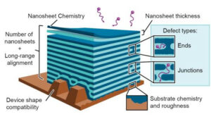
Teadlased töötasid välja uue isekoostumismeetodi mitmekihiliste 2D nanolehtede valmistamiseks
Allikasõlm: 3088801
Ajatempel: Jan 29, 2024
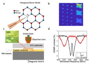
Heeliumioonide pommitamisel tekkinud kuusnurkse boornitriidi keerdumisdefektid
Allikasõlm: 2782123
Ajatempel: Juuli 24, 2023
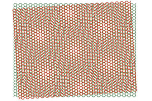
Konkreetne grafeeni ja boornitriidi "võileib" võib viia järgmise põlvkonna mikroelektroonikani
Allikasõlm: 2598354
Ajatempel: Aprill 20, 2023
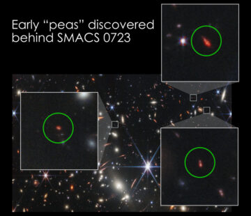
James Webbi kosmoseteleskoop paljastab seosed lähedal ja kaugel asuvate galaktikate vahel
Allikasõlm: 1889333
Ajatempel: Jan 9, 2023
Vallandab värvide häälestatavate nanoseadmete uus ajastu – kõigi aegade väikseim ümberlülitatavate värvidega valgusallikas
Allikasõlm: 2801585
Ajatempel: August 3, 2023
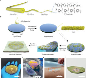
Uus üliõhuke "nahk" paindliku elektroonika jaoks tõotab edusamme meditsiiniseadmete ja proteeside vallas
Allikasõlm: 3075264
Ajatempel: Jan 20, 2024
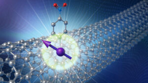
Süsiniknanotoru teeb ideaalseks koduks kvantbittide keerutamiseks
Allikasõlm: 1995470
Ajatempel: Mar 6, 2023
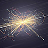
Ebatavaline aatom aitab otsida Universumi ehitusplokke
Allikasõlm: 1980749
Ajatempel: Veebruar 24, 2023
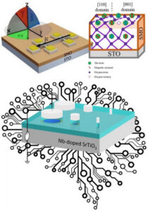
Maailma esimene universaalne metasurface antenn kõrge turvalisusega 6G side jaoks
Allikasõlm: 3013617
Ajatempel: Detsember 14, 2023